ATEVK1104 Atmel, ATEVK1104 Datasheet - Page 118
ATEVK1104
Manufacturer Part Number
ATEVK1104
Description
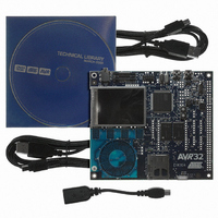
KIT DEV/EVAL FOR AVR32 AT32UC3A
Manufacturer
Atmel
Series
AVR®32r
Type
MCUr
Datasheets
1.ATAVRONE-PROBECBL.pdf
(16 pages)
2.ATEVK1104.pdf
(826 pages)
3.ATEVK1104.pdf
(90 pages)
4.ATEVK1104.pdf
(6 pages)
5.ATEVK1104.pdf
(12 pages)
Specifications of ATEVK1104
Contents
Evaluation Board, Software and Documentation
Processor To Be Evaluated
AT32UC3A3
Data Bus Width
32 bit
Interface Type
USB, SPI, USART
Silicon Manufacturer
Atmel
Core Architecture
AVR
Core Sub-architecture
AVR UC3
Silicon Core Number
AT32UC3A3256
Silicon Family Name
AVR
Kit Contents
Board CD Docs
Rohs Compliant
Yes
For Use With/related Products
AT32UC3A3
Lead Free Status / RoHS Status
Lead free / RoHS Compliant
Available stocks
Company
Part Number
Manufacturer
Quantity
Price
Company:

Part Number:
ATEVK1104
Manufacturer:
Atmel
Quantity:
135


18.4.7
18.5
32058J–AVR32–04/11
Flash commands
Writing words to a page that is not completely erased
The page buffer is also used for writes to the User page.
Write operations can be prevented by programming the Memory Protection Unit of the CPU.
Writing 8-bit and 16-bit data to the page buffer is not allowed and may lead to unpredictable
data corruption.
Page buffer write operations are performed with 4 wait states.
Writing to the page buffer can only change page buffer bits from one to zero, ie writing
0xaaaaaaaa to a page buffer location that has the value 0x00000000, will not change the page
buffer value. The only way to change a bit from zero to one, is to reset the entire page buffer
with the Clear Page Buffer command.
The page buffer is not automatically reset after a page write. The programmer should do this
manually by issuing the Clear Page Buffer flash command. This can be done after a page
write, or before the page buffer is loaded with data to be stored to the flash page.
Example: Writing a word into word address 130 of a flash with 128 words in the page buffer.
PAGEN will be updated with the value 1, and the word will be written into word 2 in the page
buffer.
This can be used for EEPROM emulation, i.e. writes with granularity of one word instead of an
entire page. Only words that are in an completely erased state (0xFFFFFFFF) can be
changed. The procedure is as follows:
The FLASHC offers a command set to manage programming of the flash memory, locking and
unlocking of regions, and full flash erasing. See chapter 18.8.3 for a complete list of
commands.
To run a command, the field CMD of the Flash Command Register (FCMD) has to be written
with the command number. As soon as the FCMD register is written, the FRDY flag is auto-
matically cleared. Once the current command is complete, the FRDY flag is automatically set.
If an interrupt has been enabled by setting the bit FRDY in FCR, the interrupt line of the flash
controller is activated. All flash commands except for Quick Page Read (QPR) will generate an
interrupt request upon completion if FRDY is set.
After a command has been written to FCMD, the programming algorithm should wait until the
command has been executed before attempting to read instructions or data from the flash or
writing to the page buffer, as the flash will be busy. The waiting can be performed either by
polling the Flash Status Register (FSR) or by waiting for the flash ready interrupt. The com-
mand written to FCMD is initiated on the first clock cycle where the HSB bus interface in
FLASHC is IDLE. The user must make sure that the access pattern to the FLASHC HSB inter-
face contains an IDLE cycle so that the command is allowed to start. Make sure that no bus
masters such as DMA controllers are performing endless burst transfers from the flash. Also,
make sure that the CPU does not perform endless burst transfers from flash. This is done by
1. Clear page buffer
2. Write to the page buffer the result of the logical bitwise AND operation between the
3. Write Page.
contents of the flash page and the new data to write. Only words that were in an
erased state can be changed from the original page.
AT32UC3A
118
Related parts for ATEVK1104
Image
Part Number
Description
Manufacturer
Datasheet
Request
R

Part Number:
Description:
DEV KIT FOR AVR/AVR32
Manufacturer:
Atmel
Datasheet:

Part Number:
Description:
INTERVAL AND WIPE/WASH WIPER CONTROL IC WITH DELAY
Manufacturer:
ATMEL Corporation
Datasheet:
Part Number:
Description:
Low-Voltage Voice-Switched IC for Hands-Free Operation
Manufacturer:
ATMEL Corporation
Datasheet:
Part Number:
Description:
MONOLITHIC INTEGRATED FEATUREPHONE CIRCUIT
Manufacturer:
ATMEL Corporation
Datasheet:
Part Number:
Description:
AM-FM Receiver IC U4255BM-M
Manufacturer:
ATMEL Corporation
Datasheet:
Part Number:
Description:
Monolithic Integrated Feature Phone Circuit
Manufacturer:
ATMEL Corporation
Datasheet:
Part Number:
Description:
Multistandard Video-IF and Quasi Parallel Sound Processing
Manufacturer:
ATMEL Corporation
Datasheet:
Part Number:
Description:
High-performance EE PLD
Manufacturer:
ATMEL Corporation
Datasheet:
Part Number:
Description:
8-bit Flash Microcontroller
Manufacturer:
ATMEL Corporation
Datasheet:
Part Number:
Description:
2-Wire Serial EEPROM
Manufacturer:
ATMEL Corporation
Datasheet: