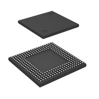
HD6417750SBP200 Renesas Electronics America, HD6417750SBP200 Datasheet - Page 615

HD6417750SBP200
Manufacturer Part Number
HD6417750SBP200
Description
IC SUPERH MPU ROMLESS 256BGA
Manufacturer
Renesas Electronics America
Series
SuperH® SH7750r
Datasheet
1.D6417750RBP240DV.pdf
(1164 pages)
Specifications of HD6417750SBP200
Core Processor
SH-4
Core Size
32-Bit
Speed
200MHz
Connectivity
EBI/EMI, FIFO, SCI, SmartCard
Peripherals
DMA, POR, WDT
Number Of I /o
28
Program Memory Type
ROMless
Ram Size
24K x 8
Voltage - Supply (vcc/vdd)
1.8 V ~ 2.07 V
Oscillator Type
External
Operating Temperature
-20°C ~ 75°C
Package / Case
256-BGA
Lead Free Status / RoHS Status
Contains lead / RoHS non-compliant
Eeprom Size
-
Program Memory Size
-
Data Converters
-
Available stocks
Company
Part Number
Manufacturer
Quantity
Price
Part Number:
HD6417750SBP200
Manufacturer:
RENESAS/瑞萨
Quantity:
20 000
- Current page: 615 of 1164
- Download datasheet (7Mb)
Section 13 Bus State Controller (BSC)
13.3.9
Byte Control SRAM Interface
The byte control SRAM interface is a memory interface that outputs a byte select strobe (WEn) in
both read and write bus cycles. It has 16 bit data pins, and can be connected to SRAM which has
an upper byte select strobe and lower byte select strobe function such as UB and LB.
Areas 1 and 4 can be designated as byte control SRAM interface. However, when these areas are
set to MPX mode, MPX mode has priority.
The byte control SRAM interface write timing is the same as for the normal SRAM interface.
In read operations, the WEn pin timing is different. In a read access, only the WE signal for the
byte being read is asserted. Assertion is synchronized with the fall of the CKIO clock, as for the
WE signal, while negation is synchronized with the rise of the CKIO clock, using the same timing
as the RD signal.
In 32-byte transfer such as a cache fill or copy-back, a total of 32 bytes are transferred
consecutively according to the set bus width. The first access is performed on the data for which
there was an access request, and the remaining accesses are performed on the data at the 32-byte
boundary. The bus is not released during this period.
Figure 13.74 shows an example of byte control SRAM connection to this LSI, and figures 13.75 to
13.77 show examples of byte control SRAM read cycle.
Rev.7.00 Oct. 10, 2008 Page 529 of 1074
REJ09B0366-0700
Related parts for HD6417750SBP200
Image
Part Number
Description
Manufacturer
Datasheet
Request
R

Part Number:
Description:
KIT STARTER FOR M16C/29
Manufacturer:
Renesas Electronics America
Datasheet:

Part Number:
Description:
KIT STARTER FOR R8C/2D
Manufacturer:
Renesas Electronics America
Datasheet:

Part Number:
Description:
R0K33062P STARTER KIT
Manufacturer:
Renesas Electronics America
Datasheet:

Part Number:
Description:
KIT STARTER FOR R8C/23 E8A
Manufacturer:
Renesas Electronics America
Datasheet:

Part Number:
Description:
KIT STARTER FOR R8C/25
Manufacturer:
Renesas Electronics America
Datasheet:

Part Number:
Description:
KIT STARTER H8S2456 SHARPE DSPLY
Manufacturer:
Renesas Electronics America
Datasheet:

Part Number:
Description:
KIT STARTER FOR R8C38C
Manufacturer:
Renesas Electronics America
Datasheet:

Part Number:
Description:
KIT STARTER FOR R8C35C
Manufacturer:
Renesas Electronics America
Datasheet:

Part Number:
Description:
KIT STARTER FOR R8CL3AC+LCD APPS
Manufacturer:
Renesas Electronics America
Datasheet:

Part Number:
Description:
KIT STARTER FOR RX610
Manufacturer:
Renesas Electronics America
Datasheet:

Part Number:
Description:
KIT STARTER FOR R32C/118
Manufacturer:
Renesas Electronics America
Datasheet:

Part Number:
Description:
KIT DEV RSK-R8C/26-29
Manufacturer:
Renesas Electronics America
Datasheet:

Part Number:
Description:
KIT STARTER FOR SH7124
Manufacturer:
Renesas Electronics America
Datasheet:

Part Number:
Description:
KIT STARTER FOR H8SX/1622
Manufacturer:
Renesas Electronics America
Datasheet:

Part Number:
Description:
KIT DEV FOR SH7203
Manufacturer:
Renesas Electronics America
Datasheet:


