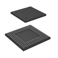
HD6417750SBP200 Renesas Electronics America, HD6417750SBP200 Datasheet - Page 476

HD6417750SBP200
Manufacturer Part Number
HD6417750SBP200
Description
IC SUPERH MPU ROMLESS 256BGA
Manufacturer
Renesas Electronics America
Series
SuperH® SH7750r
Datasheet
1.D6417750RBP240DV.pdf
(1164 pages)
Specifications of HD6417750SBP200
Core Processor
SH-4
Core Size
32-Bit
Speed
200MHz
Connectivity
EBI/EMI, FIFO, SCI, SmartCard
Peripherals
DMA, POR, WDT
Number Of I /o
28
Program Memory Type
ROMless
Ram Size
24K x 8
Voltage - Supply (vcc/vdd)
1.8 V ~ 2.07 V
Oscillator Type
External
Operating Temperature
-20°C ~ 75°C
Package / Case
256-BGA
Lead Free Status / RoHS Status
Contains lead / RoHS non-compliant
Eeprom Size
-
Program Memory Size
-
Data Converters
-
Available stocks
Company
Part Number
Manufacturer
Quantity
Price
Part Number:
HD6417750SBP200
Manufacturer:
RENESAS/瑞萨
Quantity:
20 000
- Current page: 476 of 1164
- Download datasheet (7Mb)
Section 13 Bus State Controller (BSC)
• Idle Insertion between Accesses
Read
Write
DMA read
(memory →
device)
DMA write
(device →
memory)
“DMA” in the table indicates DMA single-address transfer. DMA dual transfer is in accordance with
the CPU.
Legend:
M, D: Idle wait always inserted by WCR1
M:
D:
Notes: When synchronous DRAM is used in RAS down mode, set bits DMAIW2-DMAIW0 to 000
Rev.7.00 Oct. 10, 2008 Page 390 of 1074
REJ09B0366-0700
Preceding
Cycle
(M(1): One cycle inserted in MPX access even if WCR1 is cleared to 0)
Idle cycles according to setting of AnIW2-AnIW0 (area 0 to area 6)
Idle cycles according to setting of DMAIW2-DMAIW0
and bits A3IW2-A3IW0 to 000.
1. Inserted when device is switched
2. On the MPX interface, a WCR1 idle wait may be inserted before an access (either read
or write) to the same area after a write access. The specific conditions for idle wait
insertion in accesses to the same area are shown below.
(a) Synchronous DRAM set to RAS down mode
(b) Synchronous DRAM accessed by on-chip DMAC
Apart from use under above conditions (a) and (b), an idle wait is also inserted between
an MPX interface write access and a following access to the same area. Even under
the above conditions, an idle wait may be inserted in a same-area access following an
interface write access, depending on the synchronous DRAM pipeline access situation.
An idle wait is not inserted when the WCR1 register setting is 0. The setting for the
number of idle state cycles inserted after a power-on reset is the default value of 15 (the
maximum value), so ensure that the optimum value is set.
D
CPU DMA
Read
D
Same Area
M
M
D
CPU DMA
Write
Following Cycle
M
M
D *
1
M
M
D
CPU DMA
M
Read
M
M
M
D
Different Area
M
M
M
D
CPU DMA
Write
M
M
M
D
M (1)
*
—
—
Same
Area
MPX
Address
Output
2
Different
Area
MPX
Address
Output
M (1)
M
M (1)
D (1)
Related parts for HD6417750SBP200
Image
Part Number
Description
Manufacturer
Datasheet
Request
R

Part Number:
Description:
KIT STARTER FOR M16C/29
Manufacturer:
Renesas Electronics America
Datasheet:

Part Number:
Description:
KIT STARTER FOR R8C/2D
Manufacturer:
Renesas Electronics America
Datasheet:

Part Number:
Description:
R0K33062P STARTER KIT
Manufacturer:
Renesas Electronics America
Datasheet:

Part Number:
Description:
KIT STARTER FOR R8C/23 E8A
Manufacturer:
Renesas Electronics America
Datasheet:

Part Number:
Description:
KIT STARTER FOR R8C/25
Manufacturer:
Renesas Electronics America
Datasheet:

Part Number:
Description:
KIT STARTER H8S2456 SHARPE DSPLY
Manufacturer:
Renesas Electronics America
Datasheet:

Part Number:
Description:
KIT STARTER FOR R8C38C
Manufacturer:
Renesas Electronics America
Datasheet:

Part Number:
Description:
KIT STARTER FOR R8C35C
Manufacturer:
Renesas Electronics America
Datasheet:

Part Number:
Description:
KIT STARTER FOR R8CL3AC+LCD APPS
Manufacturer:
Renesas Electronics America
Datasheet:

Part Number:
Description:
KIT STARTER FOR RX610
Manufacturer:
Renesas Electronics America
Datasheet:

Part Number:
Description:
KIT STARTER FOR R32C/118
Manufacturer:
Renesas Electronics America
Datasheet:

Part Number:
Description:
KIT DEV RSK-R8C/26-29
Manufacturer:
Renesas Electronics America
Datasheet:

Part Number:
Description:
KIT STARTER FOR SH7124
Manufacturer:
Renesas Electronics America
Datasheet:

Part Number:
Description:
KIT STARTER FOR H8SX/1622
Manufacturer:
Renesas Electronics America
Datasheet:

Part Number:
Description:
KIT DEV FOR SH7203
Manufacturer:
Renesas Electronics America
Datasheet:


