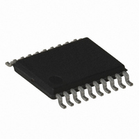
ATTINY167-15XD Atmel, ATTINY167-15XD Datasheet - Page 90

ATTINY167-15XD
Manufacturer Part Number
ATTINY167-15XD
Description
MCU AVR 16K FLASH 15MHZ 20-TSSOP
Manufacturer
Atmel
Series
AVR® ATtinyr
Datasheet
1.ATTINY167-15MD.pdf
(283 pages)
Specifications of ATTINY167-15XD
Core Processor
AVR
Core Size
8-Bit
Speed
16MHz
Connectivity
I²C, LIN, SPI, UART/USART, USI
Peripherals
Brown-out Detect/Reset, POR, PWM, Temp Sensor, WDT
Number Of I /o
16
Program Memory Size
16KB (8K x 16)
Program Memory Type
FLASH
Eeprom Size
512 x 8
Ram Size
512 x 8
Voltage - Supply (vcc/vdd)
2.7 V ~ 5.5 V
Data Converters
A/D 11x10b
Oscillator Type
Internal
Operating Temperature
-40°C ~ 150°C
Package / Case
20-TSSOP
Processor Series
ATTINY1x
Core
AVR8
Data Bus Width
8 bit
Data Ram Size
512 B
Maximum Clock Frequency
16 MHz
Maximum Operating Temperature
+ 85 C
Mounting Style
SMD/SMT
3rd Party Development Tools
EWAVR, EWAVR-BL
Development Tools By Supplier
ATAVRDRAGON, ATSTK500, ATSTK600, ATAVRISP2, ATAVRONEKIT
Minimum Operating Temperature
- 40 C
For Use With
ATSTK600-SOIC - STK600 SOCKET/ADAPTER FOR SOIC
Lead Free Status / RoHS Status
Lead free / RoHS Compliant
- Current page: 90 of 283
- Download datasheet (5Mb)
Depending on the mode of operation used, the counter is cleared, incremented, or decre-
mented at each timer clock (clk
0). clk
0 can be generated from an external or internal clock
T
T
source, selected by the Clock Select bits (CS02:0). When no clock source is selected (CS02:0
= 0) the timer is stopped. However, the TCNT0 value can be accessed by the CPU, regardless
of whether clk
0 is present or not. A CPU write overrides (has priority over) all counter clear or
T
count operations.
The counting sequence is determined by the setting of the WGM01 and WGM00 bits located
in the Timer/Counter Control Register (TCCR0A). There are close connections between how
the counter behaves (counts) and how waveforms are generated on the Output Compare out-
put OC0A. For more details about advanced counting sequences and waveform generation,
see
“Modes of Operation” on page
92.
The Timer/Counter Overflow Flag (TOV0) is set according to the mode of operation selected
by the WGM01:0 bits. TOV0 can be used for generating a CPU interrupt.
10.5
Output Compare Unit
The 8-bit comparator continuously compares TCNT0 with the Output Compare Register
(OCR0A). Whenever TCNT0 equals OCR0A, the comparator signals a match. A match will set
the Output Compare Flag (OCF0A) at the next timer clock cycle. If enabled (OCIE0A = 1), the
Output Compare Flag generates an Output Compare interrupt. The OCF0A flag is automati-
cally cleared when the interrupt is executed. Alternatively, the OCF0A flag can be cleared by
software by writing a logical one to its I/O bit location. The Waveform Generator uses the
match signal to generate an output according to operating mode set by the WGM01:0 bits and
Compare Output mode (COM0A1:0) bits. The max and bottom signals are used by the Wave-
form Generator for handling the special cases of the extreme values in some modes of
operation
(“Modes of Operation” on page
92).
Figure 10-3
shows a block diagram of the Output Compare unit.
Figure 10-3. Output Compare Unit, Block Diagram
DATA BUS
OCRnx
TCNTn
=
(8-bit Comparator )
OCFnx (Int.Req.)
top
bottom
Waveform Generator
OCnx
FOCn
WGMn1:0
COMnX1:0
ATtiny87/ATtiny167
90
7728G–AVR–06/10
Related parts for ATTINY167-15XD
Image
Part Number
Description
Manufacturer
Datasheet
Request
R

Part Number:
Description:
Manufacturer:
Atmel Corporation
Datasheet:

Part Number:
Description:
Manufacturer:
Atmel Corporation
Datasheet:

Part Number:
Description:
MCU AVR 16K FLASH 15MHZ 32-QFN
Manufacturer:
Atmel
Datasheet:

Part Number:
Description:
IC MCU AVR 16K FLASH 20TSSOP
Manufacturer:
Atmel
Datasheet:

Part Number:
Description:
MCU AVR 16K FLASH 15MHZ 32-QFN
Manufacturer:
Atmel
Datasheet:

Part Number:
Description:
MCU AVR 16K FLASH 15MHZ 20-SOIC
Manufacturer:
Atmel
Datasheet:

Part Number:
Description:
MCU AVR 16K FLASH 15MHZ 20-TSSOP
Manufacturer:
Atmel
Datasheet:

Part Number:
Description:
IC MCU AVR 16K FLASH 20SOIC
Manufacturer:
Atmel
Datasheet:


