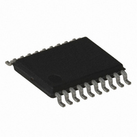
ATTINY167-15XD Atmel, ATTINY167-15XD Datasheet - Page 128

ATTINY167-15XD
Manufacturer Part Number
ATTINY167-15XD
Description
MCU AVR 16K FLASH 15MHZ 20-TSSOP
Manufacturer
Atmel
Series
AVR® ATtinyr
Datasheet
1.ATTINY167-15MD.pdf
(283 pages)
Specifications of ATTINY167-15XD
Core Processor
AVR
Core Size
8-Bit
Speed
16MHz
Connectivity
I²C, LIN, SPI, UART/USART, USI
Peripherals
Brown-out Detect/Reset, POR, PWM, Temp Sensor, WDT
Number Of I /o
16
Program Memory Size
16KB (8K x 16)
Program Memory Type
FLASH
Eeprom Size
512 x 8
Ram Size
512 x 8
Voltage - Supply (vcc/vdd)
2.7 V ~ 5.5 V
Data Converters
A/D 11x10b
Oscillator Type
Internal
Operating Temperature
-40°C ~ 150°C
Package / Case
20-TSSOP
Processor Series
ATTINY1x
Core
AVR8
Data Bus Width
8 bit
Data Ram Size
512 B
Maximum Clock Frequency
16 MHz
Maximum Operating Temperature
+ 85 C
Mounting Style
SMD/SMT
3rd Party Development Tools
EWAVR, EWAVR-BL
Development Tools By Supplier
ATAVRDRAGON, ATSTK500, ATSTK600, ATAVRISP2, ATAVRONEKIT
Minimum Operating Temperature
- 40 C
For Use With
ATSTK600-SOIC - STK600 SOCKET/ADAPTER FOR SOIC
Lead Free Status / RoHS Status
Lead free / RoHS Compliant
- Current page: 128 of 283
- Download datasheet (5Mb)
12.9.5
128
ATtiny87/ATtiny167
Phase and Frequency Correct PWM Mode
It is recommended to use the phase and frequency correct mode instead of the phase correct
mode when changing the TOP value while the Timer/Counter is running. When using a static
TOP value there are practically no differences between the two modes of operation.
In phase correct PWM mode, the compare units allow generation of PWM waveforms on the
OC1A/B pins. Setting the COM1A/B1:0 bits to two will produce a non-inverted PWM and an
inverted PWM output can be generated by setting the COM1A/B1:0 to three (See
page
the port pin is set as output (DDR_OC1A/B) and OC1A/Bi is set. The PWM waveform is gener-
ated by setting (or clearing) the OC1A/B Register at the compare match between OCR1A/B
and TCNT1 when the counter increments, and clearing (or setting) the OC1A/B Register at
compare match between OCR1A/B and TCNT1 when the counter decrements. The PWM fre-
quency for the output when using phase correct PWM can be calculated by the following
equation:
The N variable represents the prescaler divider (1, 8, 64, 256, or 1024).
The extreme values for the OCR1A/B Register represent special cases when generating a
PWM waveform output in the phase correct PWM mode. If the OCR1A/B is set equal to BOT-
TOM the output will be continuously low and if set equal to TOP the output will be continuously
high for non-inverted PWM mode. For inverted PWM the output will have the opposite logic
values.
The phase and frequency correct Pulse Width Modulation, or phase and frequency correct
PWM mode (WGM13:0 = 8 or 9) provides a high resolution phase and frequency correct PWM
waveform generation option. The phase and frequency correct PWM mode is, like the phase
correct PWM mode, based on a dual-slope operation. The counter counts repeatedly from
BOTTOM (0x0000) to TOP and then from TOP to BOTTOM. In non-inverting Compare Output
mode, the Output Compare (OC1A/B) is cleared on the compare match between TCNT1 and
OCR1A/B while upcounting, and set on the compare match while downcounting. In inverting
Compare Output mode, the operation is inverted. The dual-slope operation gives a lower max-
imum operation frequency compared to the single-slope operation. However, due to the
symmetric feature of the dual-slope PWM modes, these modes are preferred for motor control
applications.
The main difference between the phase correct, and the phase and frequency correct PWM
mode is the time the OCR1A/B Register is updated by the OCR1A/B Buffer Register, (see
ure 12-9
The PWM resolution for the phase and frequency correct PWM mode can be defined by either
ICR1 or OCR1A. The minimum resolution allowed is 2-bit (ICR1 or OCR1A set to 0x0003),
and the maximum resolution is 16-bit (ICR1 or OCR1A set to MAX). The PWM resolution in
bits can be calculated using the following equation:
133). The actual OC1A/B value will only be visible on the port pin if the data direction for
and
Figure
12-10).
R
f
PFCPWM
OCnxPCPWM
=
log
---------------------------------- -
=
log
---------------------------------
2
TOP
f
2
clk_I/O
N
+
1
TOP
7728G–AVR–06/10
Table on
Fig-
Related parts for ATTINY167-15XD
Image
Part Number
Description
Manufacturer
Datasheet
Request
R

Part Number:
Description:
Manufacturer:
Atmel Corporation
Datasheet:

Part Number:
Description:
Manufacturer:
Atmel Corporation
Datasheet:

Part Number:
Description:
MCU AVR 16K FLASH 15MHZ 32-QFN
Manufacturer:
Atmel
Datasheet:

Part Number:
Description:
IC MCU AVR 16K FLASH 20TSSOP
Manufacturer:
Atmel
Datasheet:

Part Number:
Description:
MCU AVR 16K FLASH 15MHZ 32-QFN
Manufacturer:
Atmel
Datasheet:

Part Number:
Description:
MCU AVR 16K FLASH 15MHZ 20-SOIC
Manufacturer:
Atmel
Datasheet:

Part Number:
Description:
MCU AVR 16K FLASH 15MHZ 20-TSSOP
Manufacturer:
Atmel
Datasheet:

Part Number:
Description:
IC MCU AVR 16K FLASH 20SOIC
Manufacturer:
Atmel
Datasheet:


