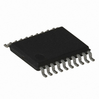
ATTINY167-15XD Atmel, ATTINY167-15XD Datasheet - Page 211

ATTINY167-15XD
Manufacturer Part Number
ATTINY167-15XD
Description
MCU AVR 16K FLASH 15MHZ 20-TSSOP
Manufacturer
Atmel
Series
AVR® ATtinyr
Datasheet
1.ATTINY167-15MD.pdf
(283 pages)
Specifications of ATTINY167-15XD
Core Processor
AVR
Core Size
8-Bit
Speed
16MHz
Connectivity
I²C, LIN, SPI, UART/USART, USI
Peripherals
Brown-out Detect/Reset, POR, PWM, Temp Sensor, WDT
Number Of I /o
16
Program Memory Size
16KB (8K x 16)
Program Memory Type
FLASH
Eeprom Size
512 x 8
Ram Size
512 x 8
Voltage - Supply (vcc/vdd)
2.7 V ~ 5.5 V
Data Converters
A/D 11x10b
Oscillator Type
Internal
Operating Temperature
-40°C ~ 150°C
Package / Case
20-TSSOP
Processor Series
ATTINY1x
Core
AVR8
Data Bus Width
8 bit
Data Ram Size
512 B
Maximum Clock Frequency
16 MHz
Maximum Operating Temperature
+ 85 C
Mounting Style
SMD/SMT
3rd Party Development Tools
EWAVR, EWAVR-BL
Development Tools By Supplier
ATAVRDRAGON, ATSTK500, ATSTK600, ATAVRISP2, ATAVRONEKIT
Minimum Operating Temperature
- 40 C
For Use With
ATSTK600-SOIC - STK600 SOCKET/ADAPTER FOR SOIC
Lead Free Status / RoHS Status
Lead free / RoHS Compliant
- Current page: 211 of 283
- Download datasheet (5Mb)
18. AnaComp - Analog Comparator
18.1
18.1.1
7728G–AVR–06/10
Register Description
ADC Control and Status Register B – ADCSRB
ADC Multiplexer
The Analog Comparator compares the input values on the positive pin (AIN1) and negative pin
(AIN0). When the voltage on the positive pin is higher than the voltage on the negative pin, the
Analog Comparator output, ACO, is set. The comparator can trigger a separate interrupt,
exclusive to the Analog Comparator. The user can select Interrupt triggering on comparator
output rise, fall or toggle. A block diagram of the comparator and its surrounding logic is shown
in
Figure 18-1. Analog Comparator Block Diagram
Notes:
• Bit 6 – ACME: Analog Comparator Multiplexer Enable
When this bit is written logic one and the ADC is switched off (ADEN in ADCSRA is zero), the
ADC multiplexer selects the positive input to the Analog Comparator. When this bit is written
logic zero, AIN1 is applied to the positive input of the Analog Comparator.
When the Analog to Digital Converter (ADC) is configured as single ended input channel, it is
possible to select any of the ADC[10..0] pins to replace the positive input to the Analog Com-
parator. The ADC multiplexer (MUX[4..0]) is used to select this input, and consequently, the
ADC must be switched off to utilize this feature.
(from ADC)
Bit
Read/Write
Initial Value
REFS0
REFS1
Output
ADEN
Figure
(1)
1. See
2. Refer to
Reference
18-1.
Internal
2.56 V
placement.
ACIRS
Table 18-2 on page 214
ACME
BIN
(PA7)
(PA6)
R
AIN1
AIN0
7
0
Figure 1-2 on page 5
2.56 V
1.28 V
0.64 V
0.32 V
ACME
R/W
6
0
ACIR0
ACIR1
ACIR1
R/W
5
0
ACD
and
and
Table 18-3 on page 214
ACIR0
AVcc
Table 9-3 on page 76
R/W
4
0
(1)(2)
ACIS1
—
R
3
0
Sensivity
Interrupt
Control
ATtiny87/ATtiny167
ACIS0
ADTS2
R/W
2
0
for Analog Comparator pin
ACIE
ADTS1
R/W
1
0
ACO
ACI
Analog Comparator
ADTS0
R/W
0
0
Interrupt
16-bit Timer/Counter
Input Capture
ADCSRB
211
Related parts for ATTINY167-15XD
Image
Part Number
Description
Manufacturer
Datasheet
Request
R

Part Number:
Description:
Manufacturer:
Atmel Corporation
Datasheet:

Part Number:
Description:
Manufacturer:
Atmel Corporation
Datasheet:

Part Number:
Description:
MCU AVR 16K FLASH 15MHZ 32-QFN
Manufacturer:
Atmel
Datasheet:

Part Number:
Description:
IC MCU AVR 16K FLASH 20TSSOP
Manufacturer:
Atmel
Datasheet:

Part Number:
Description:
MCU AVR 16K FLASH 15MHZ 32-QFN
Manufacturer:
Atmel
Datasheet:

Part Number:
Description:
MCU AVR 16K FLASH 15MHZ 20-SOIC
Manufacturer:
Atmel
Datasheet:

Part Number:
Description:
MCU AVR 16K FLASH 15MHZ 20-TSSOP
Manufacturer:
Atmel
Datasheet:

Part Number:
Description:
IC MCU AVR 16K FLASH 20SOIC
Manufacturer:
Atmel
Datasheet:


