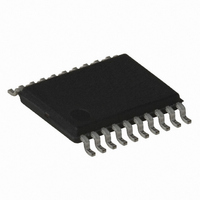
ATTINY167-15XD Atmel, ATTINY167-15XD Datasheet - Page 148

ATTINY167-15XD
Manufacturer Part Number
ATTINY167-15XD
Description
MCU AVR 16K FLASH 15MHZ 20-TSSOP
Manufacturer
Atmel
Series
AVR® ATtinyr
Datasheet
1.ATTINY167-15MD.pdf
(283 pages)
Specifications of ATTINY167-15XD
Core Processor
AVR
Core Size
8-Bit
Speed
16MHz
Connectivity
I²C, LIN, SPI, UART/USART, USI
Peripherals
Brown-out Detect/Reset, POR, PWM, Temp Sensor, WDT
Number Of I /o
16
Program Memory Size
16KB (8K x 16)
Program Memory Type
FLASH
Eeprom Size
512 x 8
Ram Size
512 x 8
Voltage - Supply (vcc/vdd)
2.7 V ~ 5.5 V
Data Converters
A/D 11x10b
Oscillator Type
Internal
Operating Temperature
-40°C ~ 150°C
Package / Case
20-TSSOP
Processor Series
ATTINY1x
Core
AVR8
Data Bus Width
8 bit
Data Ram Size
512 B
Maximum Clock Frequency
16 MHz
Maximum Operating Temperature
+ 85 C
Mounting Style
SMD/SMT
3rd Party Development Tools
EWAVR, EWAVR-BL
Development Tools By Supplier
ATAVRDRAGON, ATSTK500, ATSTK600, ATAVRISP2, ATAVRONEKIT
Minimum Operating Temperature
- 40 C
For Use With
ATSTK600-SOIC - STK600 SOCKET/ADAPTER FOR SOIC
Lead Free Status / RoHS Status
Lead free / RoHS Compliant
- Current page: 148 of 283
- Download datasheet (5Mb)
13.3
148
Data Modes
ATtiny87/ATtiny167
There are four combinations of SCK phase and polarity with respect to serial data, which are
determined by control bits CPHA and CPOL. The SPI data transfer formats are shown in
ure 13-3
SCK signal, ensuring sufficient time for data signals to stabilize. This is clearly seen by sum-
marizing
Table 13-5.
Figure 13-3. SPI Transfer Format with CPHA = 0
Figure 13-4. SPI Transfer Format with CPHA = 1
CPOL=0, CPHA=0
CPOL=0, CPHA=1
CPOL=1, CPHA=0
CPOL=1, CPHA=1
SCK (CPOL = 0)
mode 0
SCK (CPOL = 1)
mode 2
SAMPLE I
MOSI/MISO
CHANGE 0
MOSI PIN
CHANGE 0
MISO PIN
SCK (CPOL = 0)
mode 1
SCK (CPOL = 1)
mode 3
SAMPLE I
MOSI/MISO
CHANGE 0
MOSI PIN
CHANGE 0
MISO PIN
SS
SS
Table 13-2
and
MSB first (DORD = 0)
LSB first (DORD = 1)
MSB first (DORD = 0)
LSB first (DORD = 1)
Figure
CPOL Functionality
and
13-4. Data bits are shifted out and latched in on opposite edges of the
Table
MSB
LSB
MSB
LSB
13-3, as done below:
Sample (Falling)
Bit 6
Bit 1
Sample (Rising)
Leading Edge
Setup (Falling)
Setup (Rising)
Bit 6
Bit 1
Bit 5
Bit 2
Bit 5
Bit 2
Bit 4
Bit 3
Bit 4
Bit 3
Bit 3
Bit 4
Sample (Falling)
Sample (Rising)
Bit 3
Bit 4
Setup (Falling)
Setup (Rising)
Trailing Edge
Bit 2
Bit 5
Bit 2
Bit 5
Bit 1
Bit 6
Bit 1
Bit 6
LSB
MSB
7728G–AVR–06/10
LSB
MSB
SPI Mode
0
1
2
3
Fig-
Related parts for ATTINY167-15XD
Image
Part Number
Description
Manufacturer
Datasheet
Request
R

Part Number:
Description:
Manufacturer:
Atmel Corporation
Datasheet:

Part Number:
Description:
Manufacturer:
Atmel Corporation
Datasheet:

Part Number:
Description:
MCU AVR 16K FLASH 15MHZ 32-QFN
Manufacturer:
Atmel
Datasheet:

Part Number:
Description:
IC MCU AVR 16K FLASH 20TSSOP
Manufacturer:
Atmel
Datasheet:

Part Number:
Description:
MCU AVR 16K FLASH 15MHZ 32-QFN
Manufacturer:
Atmel
Datasheet:

Part Number:
Description:
MCU AVR 16K FLASH 15MHZ 20-SOIC
Manufacturer:
Atmel
Datasheet:

Part Number:
Description:
MCU AVR 16K FLASH 15MHZ 20-TSSOP
Manufacturer:
Atmel
Datasheet:

Part Number:
Description:
IC MCU AVR 16K FLASH 20SOIC
Manufacturer:
Atmel
Datasheet:


