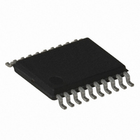
ATTINY167-15XD Atmel, ATTINY167-15XD Datasheet - Page 78

ATTINY167-15XD
Manufacturer Part Number
ATTINY167-15XD
Description
MCU AVR 16K FLASH 15MHZ 20-TSSOP
Manufacturer
Atmel
Series
AVR® ATtinyr
Datasheet
1.ATTINY167-15MD.pdf
(283 pages)
Specifications of ATTINY167-15XD
Core Processor
AVR
Core Size
8-Bit
Speed
16MHz
Connectivity
I²C, LIN, SPI, UART/USART, USI
Peripherals
Brown-out Detect/Reset, POR, PWM, Temp Sensor, WDT
Number Of I /o
16
Program Memory Size
16KB (8K x 16)
Program Memory Type
FLASH
Eeprom Size
512 x 8
Ram Size
512 x 8
Voltage - Supply (vcc/vdd)
2.7 V ~ 5.5 V
Data Converters
A/D 11x10b
Oscillator Type
Internal
Operating Temperature
-40°C ~ 150°C
Package / Case
20-TSSOP
Processor Series
ATTINY1x
Core
AVR8
Data Bus Width
8 bit
Data Ram Size
512 B
Maximum Clock Frequency
16 MHz
Maximum Operating Temperature
+ 85 C
Mounting Style
SMD/SMT
3rd Party Development Tools
EWAVR, EWAVR-BL
Development Tools By Supplier
ATAVRDRAGON, ATSTK500, ATSTK600, ATAVRISP2, ATAVRONEKIT
Minimum Operating Temperature
- 40 C
For Use With
ATSTK600-SOIC - STK600 SOCKET/ADAPTER FOR SOIC
Lead Free Status / RoHS Status
Lead free / RoHS Compliant
- Current page: 78 of 283
- Download datasheet (5Mb)
78
ATtiny87/ATtiny167
• PCINT3/ADC3/ISRC/INT1 – Port A, Bit 3
• PCINT2/ADC2/OC0A/DO/MISO – Port A, Bit 2
• PCINT1/ADC1/TXD/TXLIN – Port A, Bit 1
• PCINT0/ADC0/RXD/RXLIN – Port A, Bit 0
Table 9-4
in
PCINT3: Pin Change Interrupt, source 3.
ADC3: Analog to Digital Converter, channel 3.
ISCR: Current Source Output pin. While current is sourced by the Current Source module,
INT1: External Interrupt, source 1. The PA4 pin can serve as an external interrupt source.
PCINT2: Pin Change Interrupt, source 2.
ADC2: Analog to Digital Converter, channel 2.
OC0A: Output Compare Match A or output PWM A for Timer/Counter0. The pin has to be
DO: Three-wire Mode USI Data Output. Three-wire mode data output overrides PORTA2
MISO: Master Data input, Slave Data output pin for SPI channel. When the SPI is enabled
PCINT1: Pin Change Interrupt, source 1.
ADC1: Analog to Digital Converter, channel 1.
TXD: UART Transmit pin. When the UART transmitter is enabled, this pin is configured as an
TXLIN: LIN Transmit pin. When the LIN is enabled, this pin is configured as an output
PCINT0: Pin Change Interrupt, source 0.
ADC0: Analog to Digital Converter, channel 0.
RXD: UART Receive pin. When the UART receiver is enabled, this pin is configured as an
RXLIN: LIN Receive pin. When the LIN is enabled, this pin is configured as an input regard-
Figure 9-6 on page
Master, the data direction of this pin is controlled by DDA3. When the pin is forced by
the SPI to be an input, the pull-up can still be controlled by the PORTA3 bit.
the user can use the Analog to Digital Converter channel 4 (ADC4) to measure the pin
voltage.
configured as an output (DDA2 set
and it is driven to the port when the data direction bit DDA2 is set. PORTA2 still
enables the pull-up, if the direction is input and PORTA2 is set
as a Master, this pin is configured as an input regardless of the setting of DDA2. When
the SPI is enabled as a Salve, the data direction of this pin is controlled by DDA2.
When the pin is forced to be an input, the pull-up can still be controlled by PORTA2.
output regardless the value of DDA1. PORTA1 still enables the pull-up, if the direction
is input and PORTA2 is set
regardless the value of DDA1. PORTA1 still enables the pull-up, if the direction is input
and PORTA2 is set
input regardless of the value of DDA0. When the pin is forced to be an input, a logical
one in PORTA0 will turn on the internal pull-up.
less of the value of DDA0. When the pin is forced to be an input, a logical one in
PORTA0 will turn on the internal pull-up.
and
Table 9-5
73.
relate the alternate functions of Port A to the overriding signals shown
(
one
).
(
one
).
(
one
)
) to serve these functions.
(
one
).
7728G–AVR–06/10
Related parts for ATTINY167-15XD
Image
Part Number
Description
Manufacturer
Datasheet
Request
R

Part Number:
Description:
Manufacturer:
Atmel Corporation
Datasheet:

Part Number:
Description:
Manufacturer:
Atmel Corporation
Datasheet:

Part Number:
Description:
MCU AVR 16K FLASH 15MHZ 32-QFN
Manufacturer:
Atmel
Datasheet:

Part Number:
Description:
IC MCU AVR 16K FLASH 20TSSOP
Manufacturer:
Atmel
Datasheet:

Part Number:
Description:
MCU AVR 16K FLASH 15MHZ 32-QFN
Manufacturer:
Atmel
Datasheet:

Part Number:
Description:
MCU AVR 16K FLASH 15MHZ 20-SOIC
Manufacturer:
Atmel
Datasheet:

Part Number:
Description:
MCU AVR 16K FLASH 15MHZ 20-TSSOP
Manufacturer:
Atmel
Datasheet:

Part Number:
Description:
IC MCU AVR 16K FLASH 20SOIC
Manufacturer:
Atmel
Datasheet:


