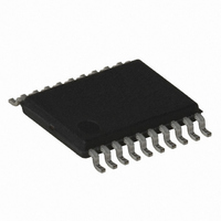
ATTINY167-15XD Atmel, ATTINY167-15XD Datasheet - Page 129

ATTINY167-15XD
Manufacturer Part Number
ATTINY167-15XD
Description
MCU AVR 16K FLASH 15MHZ 20-TSSOP
Manufacturer
Atmel
Series
AVR® ATtinyr
Datasheet
1.ATTINY167-15MD.pdf
(283 pages)
Specifications of ATTINY167-15XD
Core Processor
AVR
Core Size
8-Bit
Speed
16MHz
Connectivity
I²C, LIN, SPI, UART/USART, USI
Peripherals
Brown-out Detect/Reset, POR, PWM, Temp Sensor, WDT
Number Of I /o
16
Program Memory Size
16KB (8K x 16)
Program Memory Type
FLASH
Eeprom Size
512 x 8
Ram Size
512 x 8
Voltage - Supply (vcc/vdd)
2.7 V ~ 5.5 V
Data Converters
A/D 11x10b
Oscillator Type
Internal
Operating Temperature
-40°C ~ 150°C
Package / Case
20-TSSOP
Processor Series
ATTINY1x
Core
AVR8
Data Bus Width
8 bit
Data Ram Size
512 B
Maximum Clock Frequency
16 MHz
Maximum Operating Temperature
+ 85 C
Mounting Style
SMD/SMT
3rd Party Development Tools
EWAVR, EWAVR-BL
Development Tools By Supplier
ATAVRDRAGON, ATSTK500, ATSTK600, ATAVRISP2, ATAVRONEKIT
Minimum Operating Temperature
- 40 C
For Use With
ATSTK600-SOIC - STK600 SOCKET/ADAPTER FOR SOIC
Lead Free Status / RoHS Status
Lead free / RoHS Compliant
- Current page: 129 of 283
- Download datasheet (5Mb)
7728G–AVR–06/10
In phase and frequency correct PWM mode the counter is incremented until the counter value
matches either the value in ICR1 (WGM13:0 = 8), or the value in OCR1A (WGM13:0 = 9). The
counter has then reached the TOP and changes the count direction. The TCNT1 value will be
equal to TOP for one timer clock cycle. The timing diagram for the phase correct and fre-
quency correct PWM mode is shown on
correct PWM mode when OCR1A or ICR1 is used to define TOP. The TCNT1 value is in the
timing diagram shown as a histogram for illustrating the dual-slope operation. The diagram
includes non-inverted and inverted PWM outputs. The small horizontal line marks on the
TCNT1 slopes represent compare matches between OCR1A/B and TCNT1. The OC1A/B
interrupt flag will be set when a compare match occurs.
Figure 12-10. Phase and Frequency Correct PWM Mode, Timing Diagram
The Timer/Counter Overflow Flag (TOV1) is set at the same timer clock cycle as the OCR1A/B
Registers are updated with the double buffer value (at BOTTOM). When either OCR1A or
ICR1 is used for defining the TOP value, the OC1A or ICF1 flag set when TCNT1 has reached
TOP. The interrupt flags can then be used to generate an interrupt each time the counter
reaches the TOP or BOTTOM value.
When changing the TOP value the program must ensure that the new TOP value is higher or
equal to the value of all of the Compare Registers. If the TOP value is lower than any of the
Compare Registers, a compare match will never occur between the TCNT1 and the
OCR1A/B.
As
metrical in all periods. Since the OCR1A/B Registers are updated at BOTTOM, the length of
the rising and the falling slopes will always be equal. This gives symmetrical output pulses and
is therefore frequency correct.
Using the ICR1 Register for defining TOP works well when using fixed TOP values. By using
ICR1, the OCR1A Register is free to be used for generating a PWM output on OC1A. How-
ever, if the base PWM frequency is actively changed by changing the TOP value, using the
OCR1A as TOP is clearly a better choice due to its double buffer feature.
Figure 12-10
OCnxi
OCnxi
TCNTn
Period
shows the output generated is, in contrast to the phase correct mode, sym-
1
2
Figure
3
12-10. The figure shows phase and frequency
ATtiny87/ATtiny167
4
OCnA Interrupt Flag Set
or ICFn Interrupt Flag Set
(Interrupt on TOP)
(COMnx1:0 = 2)
(COMnx1:0 = 3)
OCRnx/TOP Update and
TOVn Interrupt Flag Set
(Interrupt on Bottom)
129
Related parts for ATTINY167-15XD
Image
Part Number
Description
Manufacturer
Datasheet
Request
R

Part Number:
Description:
Manufacturer:
Atmel Corporation
Datasheet:

Part Number:
Description:
Manufacturer:
Atmel Corporation
Datasheet:

Part Number:
Description:
MCU AVR 16K FLASH 15MHZ 32-QFN
Manufacturer:
Atmel
Datasheet:

Part Number:
Description:
IC MCU AVR 16K FLASH 20TSSOP
Manufacturer:
Atmel
Datasheet:

Part Number:
Description:
MCU AVR 16K FLASH 15MHZ 32-QFN
Manufacturer:
Atmel
Datasheet:

Part Number:
Description:
MCU AVR 16K FLASH 15MHZ 20-SOIC
Manufacturer:
Atmel
Datasheet:

Part Number:
Description:
MCU AVR 16K FLASH 15MHZ 20-TSSOP
Manufacturer:
Atmel
Datasheet:

Part Number:
Description:
IC MCU AVR 16K FLASH 20SOIC
Manufacturer:
Atmel
Datasheet:


