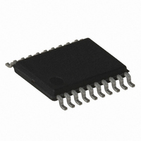
ATTINY167-15XD Atmel, ATTINY167-15XD Datasheet - Page 76

ATTINY167-15XD
Manufacturer Part Number
ATTINY167-15XD
Description
MCU AVR 16K FLASH 15MHZ 20-TSSOP
Manufacturer
Atmel
Series
AVR® ATtinyr
Datasheet
1.ATTINY167-15MD.pdf
(283 pages)
Specifications of ATTINY167-15XD
Core Processor
AVR
Core Size
8-Bit
Speed
16MHz
Connectivity
I²C, LIN, SPI, UART/USART, USI
Peripherals
Brown-out Detect/Reset, POR, PWM, Temp Sensor, WDT
Number Of I /o
16
Program Memory Size
16KB (8K x 16)
Program Memory Type
FLASH
Eeprom Size
512 x 8
Ram Size
512 x 8
Voltage - Supply (vcc/vdd)
2.7 V ~ 5.5 V
Data Converters
A/D 11x10b
Oscillator Type
Internal
Operating Temperature
-40°C ~ 150°C
Package / Case
20-TSSOP
Processor Series
ATTINY1x
Core
AVR8
Data Bus Width
8 bit
Data Ram Size
512 B
Maximum Clock Frequency
16 MHz
Maximum Operating Temperature
+ 85 C
Mounting Style
SMD/SMT
3rd Party Development Tools
EWAVR, EWAVR-BL
Development Tools By Supplier
ATAVRDRAGON, ATSTK500, ATSTK600, ATAVRISP2, ATAVRONEKIT
Minimum Operating Temperature
- 40 C
For Use With
ATSTK600-SOIC - STK600 SOCKET/ADAPTER FOR SOIC
Lead Free Status / RoHS Status
Lead free / RoHS Compliant
- Current page: 76 of 283
- Download datasheet (5Mb)
9.3.3
76
ATtiny87/ATtiny167
Alternate Functions of Port A
The Port A pins with alternate functions are shown in
Table 9-3.
Port Pin
PA7
PA6
PA5
PA4
PA3
PA2
PA1
PA0
Port A Pins Alternate Functions
Alternate Function
PCINT7 (Pin Change Interrupt 7)
ADC7 (ADC Input Channel 7)
AIN1 (Analog Comparator Positive Input)
XREF (Internal Voltage Reference Output)
AREF (External Voltage Reference Input)
PCINT6 (Pin Change Interrupt 6)
ADC6 (ADC Input Channel 6)
AIN0 (Analog Comparator Negative Input)
SS (SPI Slave Select Input)
PCINT5 (Pin Change Interrupt 5)
ADC5 (ADC Input Channel 5)
T1 (Timer/Counter1 Clock Input)
USCK (Three-wire Mode USI Alternate Clock Input)
SCL (Two-wire Mode USI Alternate Clock Input)
SCK (SPI Master Clock)
PCINT4 (Pin Change Interrupt 4)
ADC4 (ADC Input Channel 4)
ICP1 (Timer/Counter1 Input Capture Trigger)
DI (Three-wire Mode USI Alternate Data Input)
SDA (Two-wire Mode USI Alternate Data Input / Output)
MOSI (SPI Master Output / Slave Input)
PCINT3 (Pin Change Interrupt 3)
ADC3 (ADC Input Channel 3)
ISRC (Current Source Pin)
INT1 (External Interrupt1 Input)
PCINT2 (Pin Change Interrupt 2)
ADC2 (ADC Input Channel 2)
OC0A (Output Compare and PWM Output A for Timer/Counter0)
DO (Three-wire Mode USI Alternate Data Output)
MISO (SPI Master Input / Slave Output)
PCINT1 (Pin Change Interrupt 1)
ADC1 (ADC Input Channel 1)
TXD (UART Transmit Pin)
TXLIN (LIN Transmit Pin)
PCINT0 (Pin Change Interrupt 0)
ADC0 (ADC Input Channel 0)
RXD (UART Receive Pin)
RXLIN (LIN Receive Pin)
Table
9-3.
7728G–AVR–06/10
Related parts for ATTINY167-15XD
Image
Part Number
Description
Manufacturer
Datasheet
Request
R

Part Number:
Description:
Manufacturer:
Atmel Corporation
Datasheet:

Part Number:
Description:
Manufacturer:
Atmel Corporation
Datasheet:

Part Number:
Description:
MCU AVR 16K FLASH 15MHZ 32-QFN
Manufacturer:
Atmel
Datasheet:

Part Number:
Description:
IC MCU AVR 16K FLASH 20TSSOP
Manufacturer:
Atmel
Datasheet:

Part Number:
Description:
MCU AVR 16K FLASH 15MHZ 32-QFN
Manufacturer:
Atmel
Datasheet:

Part Number:
Description:
MCU AVR 16K FLASH 15MHZ 20-SOIC
Manufacturer:
Atmel
Datasheet:

Part Number:
Description:
MCU AVR 16K FLASH 15MHZ 20-TSSOP
Manufacturer:
Atmel
Datasheet:

Part Number:
Description:
IC MCU AVR 16K FLASH 20SOIC
Manufacturer:
Atmel
Datasheet:


