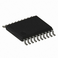
ATTINY167-15XD Atmel, ATTINY167-15XD Datasheet - Page 202

ATTINY167-15XD
Manufacturer Part Number
ATTINY167-15XD
Description
MCU AVR 16K FLASH 15MHZ 20-TSSOP
Manufacturer
Atmel
Series
AVR® ATtinyr
Datasheet
1.ATTINY167-15MD.pdf
(283 pages)
Specifications of ATTINY167-15XD
Core Processor
AVR
Core Size
8-Bit
Speed
16MHz
Connectivity
I²C, LIN, SPI, UART/USART, USI
Peripherals
Brown-out Detect/Reset, POR, PWM, Temp Sensor, WDT
Number Of I /o
16
Program Memory Size
16KB (8K x 16)
Program Memory Type
FLASH
Eeprom Size
512 x 8
Ram Size
512 x 8
Voltage - Supply (vcc/vdd)
2.7 V ~ 5.5 V
Data Converters
A/D 11x10b
Oscillator Type
Internal
Operating Temperature
-40°C ~ 150°C
Package / Case
20-TSSOP
Processor Series
ATTINY1x
Core
AVR8
Data Bus Width
8 bit
Data Ram Size
512 B
Maximum Clock Frequency
16 MHz
Maximum Operating Temperature
+ 85 C
Mounting Style
SMD/SMT
3rd Party Development Tools
EWAVR, EWAVR-BL
Development Tools By Supplier
ATAVRDRAGON, ATSTK500, ATSTK600, ATAVRISP2, ATAVRONEKIT
Minimum Operating Temperature
- 40 C
For Use With
ATSTK600-SOIC - STK600 SOCKET/ADAPTER FOR SOIC
Lead Free Status / RoHS Status
Lead free / RoHS Compliant
- Current page: 202 of 283
- Download datasheet (5Mb)
17.8
17.8.1
17.8.2
17.8.3
202
ADC Conversion Result
ATtiny87/ATtiny167
Single Ended Conversion
Unipolar Differential Conversion
Bipolar Differential Conversion
After the conversion is complete (ADIF is high), the conversion result can be found in the ADC
Result Registers (ADCL, ADCH). The form of the conversion result depends on the type of the
conversion as there are three types of conversions: single ended conversion, unipolar differ-
ential conversion and bipolar differential conversion.
For single ended conversion, the result is:
where V
Table 17-4 on page 205
0x3FF represents the selected voltage reference minus one LSB. The result is presented in
one-sided form, from 0x3FF to 0x000.
If differential channels and an unipolar input mode are used, the result is:
where V
and V
206). The voltage on the positive pin must always be larger than the voltage on the negative
pin or otherwise the voltage difference is saturated to zero. The result is presented in
one-sided form, from 0x000 (0
As default the ADC converter operates in the unipolar input mode, but the bipolar input mode
can be selected by writing the BIN bit in the ADCSRB register to one. In the bipolar input mode
two-sided voltage differences are allowed and thus the voltage on the negative input pin can
also be larger than the voltage on the positive input pin. If differential channels and a bipolar
input mode are used, the result is:
where V
and V
from 0x200 (-512
REF
REF
IN
POS
POS
the selected voltage reference (see
the selected voltage reference. The result is presented in two’s complement form,
is the voltage on the selected input pin and V
is the voltage on the positive input pin, V
is the voltage on the positive input pin, V
d
) through 0x000 (+0
and
ADC
ADC
Table 17-5 on page
d
) to 0x3FF (+1023
=
=
---------------------------------------------------------- -
-------------------------------------------------------
V
ADC
V
POS
POS
d
) to 0x1FF (+511
–
–
=
V
V
V
V
NEG
V
---------------------------- -
REF
REF
NEG
Table 17-4 on page 205
IN
V
REF
d
206). 0x000 represents analog ground, and
). The GAIN is either 8x or 20x.
1024
1024
512
NEG
NEG
REF
d
). The GAIN is either 8x or 20x.
the voltage on the negative input pin,
the voltage on the negative input pin,
the selected voltage reference (see
GAIN
GAIN
and
Table 17-5 on page
7728G–AVR–06/10
Related parts for ATTINY167-15XD
Image
Part Number
Description
Manufacturer
Datasheet
Request
R

Part Number:
Description:
Manufacturer:
Atmel Corporation
Datasheet:

Part Number:
Description:
Manufacturer:
Atmel Corporation
Datasheet:

Part Number:
Description:
MCU AVR 16K FLASH 15MHZ 32-QFN
Manufacturer:
Atmel
Datasheet:

Part Number:
Description:
IC MCU AVR 16K FLASH 20TSSOP
Manufacturer:
Atmel
Datasheet:

Part Number:
Description:
MCU AVR 16K FLASH 15MHZ 32-QFN
Manufacturer:
Atmel
Datasheet:

Part Number:
Description:
MCU AVR 16K FLASH 15MHZ 20-SOIC
Manufacturer:
Atmel
Datasheet:

Part Number:
Description:
MCU AVR 16K FLASH 15MHZ 20-TSSOP
Manufacturer:
Atmel
Datasheet:

Part Number:
Description:
IC MCU AVR 16K FLASH 20SOIC
Manufacturer:
Atmel
Datasheet:


