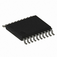
ATTINY167-15XD Atmel, ATTINY167-15XD Datasheet - Page 191

ATTINY167-15XD
Manufacturer Part Number
ATTINY167-15XD
Description
MCU AVR 16K FLASH 15MHZ 20-TSSOP
Manufacturer
Atmel
Series
AVR® ATtinyr
Datasheet
1.ATTINY167-15MD.pdf
(283 pages)
Specifications of ATTINY167-15XD
Core Processor
AVR
Core Size
8-Bit
Speed
16MHz
Connectivity
I²C, LIN, SPI, UART/USART, USI
Peripherals
Brown-out Detect/Reset, POR, PWM, Temp Sensor, WDT
Number Of I /o
16
Program Memory Size
16KB (8K x 16)
Program Memory Type
FLASH
Eeprom Size
512 x 8
Ram Size
512 x 8
Voltage - Supply (vcc/vdd)
2.7 V ~ 5.5 V
Data Converters
A/D 11x10b
Oscillator Type
Internal
Operating Temperature
-40°C ~ 150°C
Package / Case
20-TSSOP
Processor Series
ATTINY1x
Core
AVR8
Data Bus Width
8 bit
Data Ram Size
512 B
Maximum Clock Frequency
16 MHz
Maximum Operating Temperature
+ 85 C
Mounting Style
SMD/SMT
3rd Party Development Tools
EWAVR, EWAVR-BL
Development Tools By Supplier
ATAVRDRAGON, ATSTK500, ATSTK600, ATAVRISP2, ATAVRONEKIT
Minimum Operating Temperature
- 40 C
For Use With
ATSTK600-SOIC - STK600 SOCKET/ADAPTER FOR SOIC
Lead Free Status / RoHS Status
Lead free / RoHS Compliant
- Current page: 191 of 283
- Download datasheet (5Mb)
17. ADC – Analog to Digital Converter
17.1
17.2
7728G–AVR–06/10
Features
Overview
•
•
•
•
•
•
•
•
•
•
•
•
•
•
•
•
•
•
The ATtiny87/167 features a 10-bit successive approximation ADC. The ADC is connected to
a 11-channel Analog Multiplexer which allows 16 differential voltage input combinations and
11 single-ended voltage inputs constructed from the pins PA7..PA0 or PB7..PB4. The differen-
tial input is equipped with a programmable gain stage, providing amplification steps of 8x or
20x on the differential input voltage before the A/D conversion. The single-ended voltage
inputs refer to 0V (AGND).
The ADC contains a Sample and Hold circuit which ensures that the input voltage to the ADC
is held at a constant level during conversion. A block diagram of the ADC is shown in
17-1.
Internal reference voltages of nominally 1.1V or 2.56V are provided On-chip. Alternatively,
AVcc can be used as reference voltage for single ended channels. There are also options to
output the internal 1.1V or 2.56V reference voltages or to input an external voltage reference
and turn-off the internal voltage reference. These options are selected using the REFS[1:0]
bits of the ADMUX control register and using AREFEN and XREFEN bits of the AMISCR con-
trol register.
10-bit Resolution
1.0 LSB Integral Non-linearity
± 2 LSB Absolute Accuracy
13 - 260 µs Conversion Time (Low - High Resolution)
Up to 15 kSPS at Maximum Resolution
11 Multiplexed Single Ended Input Channels
8 Differential input pairs with selectable gain
Temperature sensor input channel
Voltage from Internal Current Source Driving (ISRC)
Optional Left Adjustment for ADC Result Readout
0 - AVcc ADC Input Voltage Range
Selectable 1.1V / 2.56V ADC Voltage Reference
Free Running or Single Conversion Mode
ADC Start Conversion by Auto Triggering on Interrupt Sources
Interrupt on ADC Conversion Complete
Sleep Mode Noise Canceler
Unipolar / Bipolar Input Mode
Input Polarity Reversal Mode
ATtiny87/ATtiny167
Figure
191
Related parts for ATTINY167-15XD
Image
Part Number
Description
Manufacturer
Datasheet
Request
R

Part Number:
Description:
Manufacturer:
Atmel Corporation
Datasheet:

Part Number:
Description:
Manufacturer:
Atmel Corporation
Datasheet:

Part Number:
Description:
MCU AVR 16K FLASH 15MHZ 32-QFN
Manufacturer:
Atmel
Datasheet:

Part Number:
Description:
IC MCU AVR 16K FLASH 20TSSOP
Manufacturer:
Atmel
Datasheet:

Part Number:
Description:
MCU AVR 16K FLASH 15MHZ 32-QFN
Manufacturer:
Atmel
Datasheet:

Part Number:
Description:
MCU AVR 16K FLASH 15MHZ 20-SOIC
Manufacturer:
Atmel
Datasheet:

Part Number:
Description:
MCU AVR 16K FLASH 15MHZ 20-TSSOP
Manufacturer:
Atmel
Datasheet:

Part Number:
Description:
IC MCU AVR 16K FLASH 20SOIC
Manufacturer:
Atmel
Datasheet:


