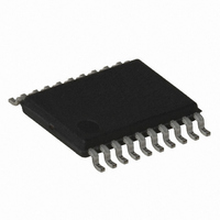
ATTINY167-15XD Atmel, ATTINY167-15XD Datasheet - Page 46

ATTINY167-15XD
Manufacturer Part Number
ATTINY167-15XD
Description
MCU AVR 16K FLASH 15MHZ 20-TSSOP
Manufacturer
Atmel
Series
AVR® ATtinyr
Datasheet
1.ATTINY167-15MD.pdf
(283 pages)
Specifications of ATTINY167-15XD
Core Processor
AVR
Core Size
8-Bit
Speed
16MHz
Connectivity
I²C, LIN, SPI, UART/USART, USI
Peripherals
Brown-out Detect/Reset, POR, PWM, Temp Sensor, WDT
Number Of I /o
16
Program Memory Size
16KB (8K x 16)
Program Memory Type
FLASH
Eeprom Size
512 x 8
Ram Size
512 x 8
Voltage - Supply (vcc/vdd)
2.7 V ~ 5.5 V
Data Converters
A/D 11x10b
Oscillator Type
Internal
Operating Temperature
-40°C ~ 150°C
Package / Case
20-TSSOP
Processor Series
ATTINY1x
Core
AVR8
Data Bus Width
8 bit
Data Ram Size
512 B
Maximum Clock Frequency
16 MHz
Maximum Operating Temperature
+ 85 C
Mounting Style
SMD/SMT
3rd Party Development Tools
EWAVR, EWAVR-BL
Development Tools By Supplier
ATAVRDRAGON, ATSTK500, ATSTK600, ATAVRISP2, ATAVRONEKIT
Minimum Operating Temperature
- 40 C
For Use With
ATSTK600-SOIC - STK600 SOCKET/ADAPTER FOR SOIC
Lead Free Status / RoHS Status
Lead free / RoHS Compliant
- Current page: 46 of 283
- Download datasheet (5Mb)
5.8.6
5.8.7
5.8.8
5.9
5.9.1
46
Register Description
ATtiny87/ATtiny167
Watchdog Timer
Port Pins
On-chip Debug System
SMCR – Sleep Mode Control Register
If the Watchdog Timer is not needed in the application, the module should be turned off. If the
Watchdog Timer is enabled, it will be enabled in all sleep modes and hence always consume
power. In the deeper sleep modes, this will contribute significantly to the total current con-
sumption. Refer to
the Watchdog Timer.
When entering a sleep mode, all port pins should be configured to use minimum power. The
most important is then to ensure that no pins drive resistive loads. In sleep modes where both
the I/O clock (clk
be disabled. This ensures that no power is consumed by the input logic when not needed. In
some cases, the input logic is needed for detecting wake-up conditions, and it will then be
enabled. Refer to the section
72
left floating or have an analog signal level close to Vcc/2, the input buffer will use excessive
power.
For analog input pins, the digital input buffer should be disabled at all times. An analog signal
level close to Vcc/2 on an input pin can cause significant current even in active mode. Digital
input buffers can be disabled by writing to the Digital Input Disable Registers (DIDR1 and
DIDR0). Refer to
Section 17.11.5 “DIDR0 – Digital Input Disable Register 0” on page 209
If the On-chip debug system is enabled by the DWEN Fuse and the chip enters sleep mode,
the main clock source is enabled and hence always consumes power. In the deeper sleep
modes, this will contribute significantly to the total current consumption.
The Sleep Mode Control Register contains control bits for power management.
• Bits 7..3 Res: Reserved Bits
These bits are unused bits in the ATtiny87/167, and will always read as zero.
• Bits 2..1 – SM1..0: Sleep Mode Select Bits 1, and 0
These bits select between the four available sleep modes as shown in
Bit
Read/Write
Initial Value
for details on which pins are enabled. If the input buffer is enabled and the input signal is
I/O
R
7
–
0
Section 17.11.6 “DIDR1 – Digital Input Disable Register 1” on page 210
) and the ADC clock (clk
Section 6.3 “Watchdog Timer” on page 53
R
6
–
0
Section 9.2.6 “Digital Input Enable and Sleep Modes” on page
R
5
–
0
ADC
R
4
–
0
) are stopped, the input buffers of the device will
R
3
–
0
SM1
R/W
2
0
for details on how to configure
SM0
R/W
1
0
Table
for details.
5-2.
R/W
SE
0
0
7728G–AVR–06/10
SMCR
and
Related parts for ATTINY167-15XD
Image
Part Number
Description
Manufacturer
Datasheet
Request
R

Part Number:
Description:
Manufacturer:
Atmel Corporation
Datasheet:

Part Number:
Description:
Manufacturer:
Atmel Corporation
Datasheet:

Part Number:
Description:
MCU AVR 16K FLASH 15MHZ 32-QFN
Manufacturer:
Atmel
Datasheet:

Part Number:
Description:
IC MCU AVR 16K FLASH 20TSSOP
Manufacturer:
Atmel
Datasheet:

Part Number:
Description:
MCU AVR 16K FLASH 15MHZ 32-QFN
Manufacturer:
Atmel
Datasheet:

Part Number:
Description:
MCU AVR 16K FLASH 15MHZ 20-SOIC
Manufacturer:
Atmel
Datasheet:

Part Number:
Description:
MCU AVR 16K FLASH 15MHZ 20-TSSOP
Manufacturer:
Atmel
Datasheet:

Part Number:
Description:
IC MCU AVR 16K FLASH 20SOIC
Manufacturer:
Atmel
Datasheet:


