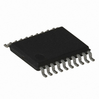
ATTINY167-15XD Atmel, ATTINY167-15XD Datasheet - Page 220

ATTINY167-15XD
Manufacturer Part Number
ATTINY167-15XD
Description
MCU AVR 16K FLASH 15MHZ 20-TSSOP
Manufacturer
Atmel
Series
AVR® ATtinyr
Datasheet
1.ATTINY167-15MD.pdf
(283 pages)
Specifications of ATTINY167-15XD
Core Processor
AVR
Core Size
8-Bit
Speed
16MHz
Connectivity
I²C, LIN, SPI, UART/USART, USI
Peripherals
Brown-out Detect/Reset, POR, PWM, Temp Sensor, WDT
Number Of I /o
16
Program Memory Size
16KB (8K x 16)
Program Memory Type
FLASH
Eeprom Size
512 x 8
Ram Size
512 x 8
Voltage - Supply (vcc/vdd)
2.7 V ~ 5.5 V
Data Converters
A/D 11x10b
Oscillator Type
Internal
Operating Temperature
-40°C ~ 150°C
Package / Case
20-TSSOP
Processor Series
ATTINY1x
Core
AVR8
Data Bus Width
8 bit
Data Ram Size
512 B
Maximum Clock Frequency
16 MHz
Maximum Operating Temperature
+ 85 C
Mounting Style
SMD/SMT
3rd Party Development Tools
EWAVR, EWAVR-BL
Development Tools By Supplier
ATAVRDRAGON, ATSTK500, ATSTK600, ATAVRISP2, ATAVRONEKIT
Minimum Operating Temperature
- 40 C
For Use With
ATSTK600-SOIC - STK600 SOCKET/ADAPTER FOR SOIC
Lead Free Status / RoHS Status
Lead free / RoHS Compliant
- Current page: 220 of 283
- Download datasheet (5Mb)
20.2.2
20.2.3
220
ATtiny87/ATtiny167
EEPROM Write Prevents Writing to SPMCSR
Reading the Fuse and Lock Bits from Software
• Bit 0 – SPMEN: Self Programming Enable
This bit enables the SPM instruction for the next four clock cycles. If written to one together
with either SIGRD, CTPB, RFLB, PGWRT, or PGERS, the following SPM instruction will have
a special meaning, see description above. If only SPMEN is written, the following SPM instruc-
tion will store the value in R1:R0 in the temporary page buffer addressed by the Z-pointer. The
LSB of the Z-pointer is ignored. The SPMEN bit will auto-clear upon completion of an SPM
instruction, or if no SPM instruction is executed within four clock cycles. During Page Erase
and Page Write, the SPMEN bit remains high until the operation is completed.
Writing any other combination than “10 0001
b
Note:
Note that an EEPROM write operation will block all software programming to Flash. Reading
the Fuses and Lock bits from software will also be prevented during the EEPROM write opera-
tion. It is recommended that the user checks the status bit (EEPE) in the EECR Register and
verifies that the bit is cleared before writing to the SPMCSR Register.
It is possible to read both the Fuse and Lock bits from software. To read the Lock bits, load the
Z-pointer with 0x0001 and set the RFLB and SPMEN bits in SPMCSR. When an LPM instruc-
tion is executed within three CPU cycles after the RFLB and SPMEN bits are set in SPMCSR,
the value of the Lock bits will be loaded in the destination register. The RFLB and SPMEN bits
will auto-clear upon completion of reading the Lock bits or if no LPM instruction is executed
within three CPU cycles or no SPM instruction is executed within four CPU cycles. When
RFLB and SPMEN are cleared, LPM will work as described in the Instruction set Manual.
The algorithm for reading the Fuse Low byte is similar to the one described above for reading
the Lock bits. To read the Fuse Low byte, load the Z-pointer with 0x0000 and set the RFLB
and SPMEN bits in SPMCSR. When an LPM instruction is executed within three cycles after
the RFLB and SPMEN bits are set in the SPMCSR, the value of the Fuse Low byte (FLB) will
be loaded in the destination register as shown below. See
detailed description and mapping of the Fuse Low byte.
Similarly, when reading the Fuse High byte (FHB), load 0x0003 in the Z-pointer. When an
LPM instruction is executed within three cycles after the RFLB and SPMEN bits are set in the
SPMCSR, the value of the Fuse High byte will be loaded in the destination register as shown
below. See
byte.
Bit
Rd (Z=0x0001)
Bit
Rd (Z=0x0000)
Bit
Rd (Z=0x0003)
” or “00 0001
Only one SPM instruction should be active at any time.
Table 21-4 on page 226
b
” in the lower six bits will have no effect.
FHB7
FLB7
7
–
7
7
FHB6
FLB6
6
–
6
6
FHB5
FLB5
5
–
5
5
for detailed description and mapping of the Fuse High
FHB4
FLB4
4
–
4
4
b
”, “01 0001
FHB3
FLB3
3
–
3
3
b
”, “00 1001
FHB2
FLB2
2
–
2
2
Table 21-5 on page 227
b
FHB1
FLB1
LB2
”, “00 0101
1
1
1
FHB0
FLB0
LB1
7728G–AVR–06/10
0
0
0
b
”, “00 0011
for a
Related parts for ATTINY167-15XD
Image
Part Number
Description
Manufacturer
Datasheet
Request
R

Part Number:
Description:
Manufacturer:
Atmel Corporation
Datasheet:

Part Number:
Description:
Manufacturer:
Atmel Corporation
Datasheet:

Part Number:
Description:
MCU AVR 16K FLASH 15MHZ 32-QFN
Manufacturer:
Atmel
Datasheet:

Part Number:
Description:
IC MCU AVR 16K FLASH 20TSSOP
Manufacturer:
Atmel
Datasheet:

Part Number:
Description:
MCU AVR 16K FLASH 15MHZ 32-QFN
Manufacturer:
Atmel
Datasheet:

Part Number:
Description:
MCU AVR 16K FLASH 15MHZ 20-SOIC
Manufacturer:
Atmel
Datasheet:

Part Number:
Description:
MCU AVR 16K FLASH 15MHZ 20-TSSOP
Manufacturer:
Atmel
Datasheet:

Part Number:
Description:
IC MCU AVR 16K FLASH 20SOIC
Manufacturer:
Atmel
Datasheet:


