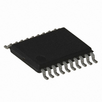
ATTINY167-15XD Atmel, ATTINY167-15XD Datasheet - Page 118

ATTINY167-15XD
Manufacturer Part Number
ATTINY167-15XD
Description
MCU AVR 16K FLASH 15MHZ 20-TSSOP
Manufacturer
Atmel
Series
AVR® ATtinyr
Datasheet
1.ATTINY167-15MD.pdf
(283 pages)
Specifications of ATTINY167-15XD
Core Processor
AVR
Core Size
8-Bit
Speed
16MHz
Connectivity
I²C, LIN, SPI, UART/USART, USI
Peripherals
Brown-out Detect/Reset, POR, PWM, Temp Sensor, WDT
Number Of I /o
16
Program Memory Size
16KB (8K x 16)
Program Memory Type
FLASH
Eeprom Size
512 x 8
Ram Size
512 x 8
Voltage - Supply (vcc/vdd)
2.7 V ~ 5.5 V
Data Converters
A/D 11x10b
Oscillator Type
Internal
Operating Temperature
-40°C ~ 150°C
Package / Case
20-TSSOP
Processor Series
ATTINY1x
Core
AVR8
Data Bus Width
8 bit
Data Ram Size
512 B
Maximum Clock Frequency
16 MHz
Maximum Operating Temperature
+ 85 C
Mounting Style
SMD/SMT
3rd Party Development Tools
EWAVR, EWAVR-BL
Development Tools By Supplier
ATAVRDRAGON, ATSTK500, ATSTK600, ATAVRISP2, ATAVRONEKIT
Minimum Operating Temperature
- 40 C
For Use With
ATSTK600-SOIC - STK600 SOCKET/ADAPTER FOR SOIC
Lead Free Status / RoHS Status
Lead free / RoHS Compliant
- Current page: 118 of 283
- Download datasheet (5Mb)
12.6.1
12.6.2
12.6.3
118
ATtiny87/ATtiny167
Input Capture Trigger Source
Noise Canceler
Using the Input Capture Unit
Register. When writing the ICR1 Register the high byte must be written to the ICR1H I/O loca-
tion before the low byte is written to ICR1L.
For more information on how to access the 16-bit registers refer to
ters” on page
The main trigger source for the Input Capture unit is the Input Capture pin (ICP1). Only
Timer/Counter1 can alternatively use the Analog Comparator output as trigger source for the
Input Capture unit. The Analog Comparator is selected as trigger source by setting the Analog
Comparator Input Capture (ACIC) bit in the Analog Comparator Control and Status Register
(ACSR). Be aware that changing trigger source can trigger a capture. The Input Capture Flag
must therefore be cleared after the change.
Both the Input Capture pin (ICP1) and the Analog Comparator output (ACO) inputs are sam-
pled using the same technique as for the T1 pin
is also identical. However, when the noise canceler is enabled, additional logic is inserted
before the edge detector, which increases the delay by four system clock cycles. Note that the
input of the noise canceler and edge detector is always enabled unless the Timer/Counter is
set in a Waveform Generation mode that uses ICR1 to define TOP.
An Input Capture can be triggered by software by controlling the port of the ICP1 pin.
The noise canceler improves noise immunity by using a simple digital filtering scheme. The
noise canceler input is monitored over four samples, and all four must be equal for changing
the output that in turn is used by the edge detector.
The noise canceler is enabled by setting the Input Capture Noise Canceler (ICNC1) bit in
Timer/Counter Control Register B (TCCR1B). When enabled the noise canceler introduces
additional four system clock cycles of delay from a change applied to the input, to the update
of the ICR1 Register. The noise canceler uses the system clock and is therefore not affected
by the prescaler.
The main challenge when using the Input Capture unit is to assign enough processor capacity
for handling the incoming events. The time between two events is critical. If the processor has
not read the captured value in the ICR1 Register before the next event occurs, the ICR1 will
be overwritten with a new value. In this case the result of the capture will be incorrect.
When using the Input Capture interrupt, the ICR1 Register should be read as early in the inter-
rupt handler routine as possible. Even though the Input Capture interrupt has relatively high
priority, the maximum interrupt response time is dependent on the maximum number of clock
cycles it takes to handle any of the other interrupt requests.
Using the Input Capture unit in any mode of operation when the TOP value (resolution) is
actively changed during operation, is not recommended.
Measurement of an external signal’s duty cycle requires that the trigger edge is changed after
each capture. Changing the edge sensing must be done as early as possible after the ICR1
Register has been read. After a change of the edge, the Input Capture Flag (ICF1) must be
cleared by software (writing a logical one to the I/O bit location). For measuring frequency
only, the clearing of the ICF1 flag is not required (if an interrupt handler is used).
112.
(Figure 11-1 on page
“Accessing 16-bit Regis-
107). The edge detector
7728G–AVR–06/10
Related parts for ATTINY167-15XD
Image
Part Number
Description
Manufacturer
Datasheet
Request
R

Part Number:
Description:
Manufacturer:
Atmel Corporation
Datasheet:

Part Number:
Description:
Manufacturer:
Atmel Corporation
Datasheet:

Part Number:
Description:
MCU AVR 16K FLASH 15MHZ 32-QFN
Manufacturer:
Atmel
Datasheet:

Part Number:
Description:
IC MCU AVR 16K FLASH 20TSSOP
Manufacturer:
Atmel
Datasheet:

Part Number:
Description:
MCU AVR 16K FLASH 15MHZ 32-QFN
Manufacturer:
Atmel
Datasheet:

Part Number:
Description:
MCU AVR 16K FLASH 15MHZ 20-SOIC
Manufacturer:
Atmel
Datasheet:

Part Number:
Description:
MCU AVR 16K FLASH 15MHZ 20-TSSOP
Manufacturer:
Atmel
Datasheet:

Part Number:
Description:
IC MCU AVR 16K FLASH 20SOIC
Manufacturer:
Atmel
Datasheet:


