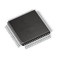
Z16FMC32AG20SG Zilog, Z16FMC32AG20SG Datasheet - Page 320

Z16FMC32AG20SG
Manufacturer Part Number
Z16FMC32AG20SG
Description
Microcontrollers (MCU) 16BIT 32K FL 2K RAM 2UART 12CH 10BIT A/D
Manufacturer
Zilog
Series
Z16FMCr
Datasheet
1.Z16FMC28AG20_EG.pdf
(341 pages)
Specifications of Z16FMC32AG20SG
Processor Series
Z16FMC
Core
ZNEO
Data Bus Width
16 bit
Program Memory Type
Flash
Program Memory Size
32 KB
Data Ram Size
2 KB
Interface Type
I2C, SPI, UART
Maximum Clock Frequency
20 MHz
Number Of Programmable I/os
46
Operating Supply Voltage
2.7 V to 3.6 V
Maximum Operating Temperature
+ 70 C
Mounting Style
SMD/SMT
Package / Case
LQFP-64
Development Tools By Supplier
Z16FMC28200KITG
Minimum Operating Temperature
0 C
Core Processor
ZNEO
Core Size
16-Bit
Speed
20MHz
Connectivity
I²C, IrDA, LIN, SPI, UART/USART
Peripherals
Brown-out Detect/Reset, DMA, POR, PWM, WDT
Number Of I /o
46
Eeprom Size
-
Ram Size
4K x 8
Voltage - Supply (vcc/vdd)
2.7 V ~ 3.6 V
Data Converters
A/D 12x10b
Oscillator Type
Internal
Operating Temperature
0°C ~ 70°C
Lead Free Status / Rohs Status
Details
Available stocks
Company
Part Number
Manufacturer
Quantity
Price
Company:
Part Number:
Z16FMC32AG20SG
Manufacturer:
Zilog
Quantity:
160
- Current page: 320 of 341
- Download datasheet (21Mb)
Table 170. POR and VBO Electrical Characteristics and Timing (Continued)
.
Table 171. Reset and Stop Mode Recovery Pin Timing
Table 172. Flash Memory Electrical Characteristics and Timing
PS028702-1210
Symbol
T
T
T
I
Note:
Symbol
T
T
Parameter
Flash Byte Read Time
Flash Byte Program Time
Flash Page Erase Time
Flash Mass Erase Time
CC
POR
VBO
RAMP
RESET
SMR
1. Data in the typical column is from characterization at 3.3 V and 0°C. These values are provided for design guid-
ance only and are not tested in production.
Parameter
Power-on reset digital
delay
Voltage Brownout pulse
rejection period
Time for V
from V
ensure valid Reset
Supply current
Parameter
RESET pin assertion to
initiate a System Reset
Stop Mode Recovery pin
Pulse Rejection Period
Table 171 lists the Reset and Stop Mode Recovery pin timing.
Table 172 lists the Flash Memory electrical characteristics and timing.
SS
to V
DD
to transition
POR
to
Min
200
50
20
10
T
A
V
0.10
Min
Min
DD
= –40°C to 105°C
10
—
—
T
T
4
P R E L I M I N A R Y
A
A
= 2.7 to 3.6 V
= –40°C to 105°C
= –40°C to 105°C
Typ
—
—
—
—
Typ
Typ
500
12
10
20
—
–
1
Max
40
—
—
—
Max
Max
100
—
—
40
–
Z16FMC Series Motor Control MCUs
Units Notes
ms
ms
ns
µs
Units
Units
T
ms
ms
µA
µs
ns
CLK
Conditions
66 IPO cycles
V
Reset
V
Conditions
Not in STOP Mode. T
System Clock period.
RESET, DBG and GPIO
pins configured as SMR
sources.
DD
DD
Product Specification
Electrical Characteristics
< V
= 3.3 V
VBO
to generate a
CLK
=
298
Related parts for Z16FMC32AG20SG
Image
Part Number
Description
Manufacturer
Datasheet
Request
R

Part Number:
Description:
Microcontrollers (MCU) 16BIT 128K FL 4KRAM 2UART 12CH 10BIT A/D
Manufacturer:
Zilog
Datasheet:

Part Number:
Description:
Microcontrollers (MCU) 16BIT 64K FL 4K RAM 2UART 12CH 10BIT A/D
Manufacturer:
Zilog
Datasheet:

Part Number:
Description:
Microcontrollers (MCU) 16BIT 32K FL 2K RAM 2UART 12CH 10BIT A/D
Manufacturer:
Zilog
Datasheet:

Part Number:
Description:
Microcontrollers (MCU) 16BIT 64K FL 4K RAM 2UART 12CH 10BIT A/D
Manufacturer:
Zilog
Datasheet:

Part Number:
Description:
Microcontrollers (MCU) 16BIT 128K FL 4KRAM 2UART 12CH 10BIT A/D
Manufacturer:
Zilog

Part Number:
Description:
Communication Controllers, ZILOG INTELLIGENT PERIPHERAL CONTROLLER (ZIP)
Manufacturer:
Zilog, Inc.
Datasheet:

Part Number:
Description:
KIT DEV FOR Z8 ENCORE 16K TO 64K
Manufacturer:
Zilog
Datasheet:

Part Number:
Description:
KIT DEV Z8 ENCORE XP 28-PIN
Manufacturer:
Zilog
Datasheet:

Part Number:
Description:
DEV KIT FOR Z8 ENCORE 8K/4K
Manufacturer:
Zilog
Datasheet:

Part Number:
Description:
KIT DEV Z8 ENCORE XP 28-PIN
Manufacturer:
Zilog
Datasheet:

Part Number:
Description:
DEV KIT FOR Z8 ENCORE 4K TO 8K
Manufacturer:
Zilog
Datasheet:

Part Number:
Description:
CMOS Z8 microcontroller. ROM 16 Kbytes, RAM 256 bytes, speed 16 MHz, 32 lines I/O, 3.0V to 5.5V
Manufacturer:
Zilog, Inc.
Datasheet:

Part Number:
Description:
Low-cost microcontroller. 512 bytes ROM, 61 bytes RAM, 8 MHz
Manufacturer:
Zilog, Inc.
Datasheet:

Part Number:
Description:
Z8 4K OTP Microcontroller
Manufacturer:
Zilog, Inc.
Datasheet:


