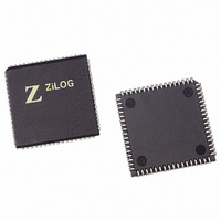
Z16C3516VSG Zilog, Z16C3516VSG Datasheet - Page 73

Z16C3516VSG
Manufacturer Part Number
Z16C3516VSG
Description
IC 16MHZ Z8500 CMOS ISCC 68-PLCC
Manufacturer
Zilog
Series
IUSC™r
Specifications of Z16C3516VSG
Controller Type
Serial Communications Controller (SCC)
Interface
USB
Voltage - Supply
4.75 V ~ 5.25 V
Current - Supply
50mA
Operating Temperature
0°C ~ 70°C
Mounting Type
Surface Mount
Package / Case
68-LCC (J-Lead)
Lead Free Status / RoHS Status
Lead free / RoHS Compliant
Other names
269-4690-5
Z16C3516VSG
Z16C3516VSG
Available stocks
Company
Part Number
Manufacturer
Quantity
Price
Company:
Part Number:
Z16C3516VSG
Manufacturer:
INTEL
Quantity:
6 219
- Current page: 73 of 268
- Download datasheet (3Mb)
UM011001-0601
5.4.9 Write Register 8 (Transmit Buffer)
WR8 is the transmit buffer register.
5.4.10 Write Register 9 (Master Interrupt
Control)
WR9 is the Master Interrupt Control register and contains
the Reset command bits. Only one WR9 exists in the ISCC
and can be accessed from either channel. The Interrupt
control bits can be programmed at the same time as the Re-
set command because these bits are only reset by a hard-
ware reset. Bit positions for WR9 are shown in Figure 5-10.
Write Register 9
D7
0
0
1
1
Sync7
Sync5
Sync15
Sync11
D6
0
1
0
1
0
D5 D4 D3 D2 D1 D0
No Reset
Channel Reset B
Channel Reset A
Force Hardware Reset
Figure 5-10. Write Register 9
Sync6
Sync4
Sync14
Sync10
1
Sync5
Sync3
Sync13
Sync9
Write Register 7
D7
1
D6
D5 D4 D3 D2 D1 D0
Sync4
Sync2
Sync12
Sync8
1
VIS
NV
DLC
MIE
Status High/Status Lo
0
Sync3
Sync1
Sync11
Sync 7
1
Figure 5-9. Write Register 7
P R E L I M I N A R Y
Sync2
Sync0
Sync10
Sync 6
1
Sync1
x
Sync9
Sync 5
Bit 7 and 6 are the Reset Command Bits
Together, these bits select one of the reset commands for
the SCC cell. Setting either of these bits to “1” disables
both the receiver and the transmitter in the corresponding
channel, forces TxD for that channel marking, forces the
modem control signals High in that channel, resets all IPs
and IUSs and disables all interrupts in that channel. Four
extra PCLK cycles must be allowed beyond the usual cycle
time after any of the active reset commands is issued be-
fore any additional commands or controls are written to the
channel affected. In the non-multiplexed bus mode, four
extra PCLK cycles must be allowed beyond the usual cycle
time before any additional command or controls are written
to the SCC cell.
Bit combination 00 is a Null Command. This command has
no effect. It is used when a write to WR9 is necessary for
some reason other than an SCC cell Reset command.
Bit combination 01 is the Channel Reset B Command. Is-
suing this command causes a channel reset to be per-
formed on Channel B.
Bit combination 10 is the Channel Reset A Command. Is-
suing this command causes a channel reset to be per-
formed on Channel A.
Bit combination 11 is the Force Hardware Reset Com-
mand. The effects of this command are identical to those
of a hardware reset, except that the Shift Right/Shift Left bit
is not changed and the MIE, Status High/Status Low and
DLC bits take the programmed values that accompany this
command.
Bit 5 is not used and must be programmed “0.”
1
Sync0
x
Sync8
Sync4
0
Monosync, 8 Bits
Monosync, 6 Bits
Bisync, 16 Bits
Bisync, 12 Bits
SDLC
Z16C35ISCC™ User’s Manual
Register Descriptions
5-13
5
Related parts for Z16C3516VSG
Image
Part Number
Description
Manufacturer
Datasheet
Request
R

Part Number:
Description:
CMOS ISCC INTEGRATED SERIAL COMMUNICATIONS CONTROLLER
Manufacturer:
ZILOG [Zilog, Inc.]
Datasheet:

Part Number:
Description:
Communication Controllers, ZILOG INTELLIGENT PERIPHERAL CONTROLLER (ZIP)
Manufacturer:
Zilog, Inc.
Datasheet:

Part Number:
Description:
KIT DEV FOR Z8 ENCORE 16K TO 64K
Manufacturer:
Zilog
Datasheet:

Part Number:
Description:
KIT DEV Z8 ENCORE XP 28-PIN
Manufacturer:
Zilog
Datasheet:

Part Number:
Description:
DEV KIT FOR Z8 ENCORE 8K/4K
Manufacturer:
Zilog
Datasheet:

Part Number:
Description:
KIT DEV Z8 ENCORE XP 28-PIN
Manufacturer:
Zilog
Datasheet:

Part Number:
Description:
DEV KIT FOR Z8 ENCORE 4K TO 8K
Manufacturer:
Zilog
Datasheet:

Part Number:
Description:
CMOS Z8 microcontroller. ROM 16 Kbytes, RAM 256 bytes, speed 16 MHz, 32 lines I/O, 3.0V to 5.5V
Manufacturer:
Zilog, Inc.
Datasheet:

Part Number:
Description:
Low-cost microcontroller. 512 bytes ROM, 61 bytes RAM, 8 MHz
Manufacturer:
Zilog, Inc.
Datasheet:

Part Number:
Description:
Z8 4K OTP Microcontroller
Manufacturer:
Zilog, Inc.
Datasheet:

Part Number:
Description:
CMOS SUPER8 ROMLESS MCU
Manufacturer:
Zilog, Inc.
Datasheet:

Part Number:
Description:
SL1866 CMOSZ8 OTP Microcontroller
Manufacturer:
Zilog, Inc.
Datasheet:

Part Number:
Description:
SL1866 CMOSZ8 OTP Microcontroller
Manufacturer:
Zilog, Inc.
Datasheet:

Part Number:
Description:
OTP (KB) = 1, RAM = 125, Speed = 12, I/O = 14, 8-bit Timers = 2, Comm Interfaces Other Features = Por, LV Protect, Voltage = 4.5-5.5V
Manufacturer:
Zilog, Inc.
Datasheet:


