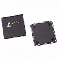
Z16C3516VSG Zilog, Z16C3516VSG Datasheet - Page 31

Z16C3516VSG
Manufacturer Part Number
Z16C3516VSG
Description
IC 16MHZ Z8500 CMOS ISCC 68-PLCC
Manufacturer
Zilog
Series
IUSC™r
Specifications of Z16C3516VSG
Controller Type
Serial Communications Controller (SCC)
Interface
USB
Voltage - Supply
4.75 V ~ 5.25 V
Current - Supply
50mA
Operating Temperature
0°C ~ 70°C
Mounting Type
Surface Mount
Package / Case
68-LCC (J-Lead)
Lead Free Status / RoHS Status
Lead free / RoHS Compliant
Other names
269-4690-5
Z16C3516VSG
Z16C3516VSG
Available stocks
Company
Part Number
Manufacturer
Quantity
Price
Company:
Part Number:
Z16C3516VSG
Manufacturer:
INTEL
Quantity:
6 219
- Current page: 31 of 268
- Download datasheet (3Mb)
UM011001-0601
3.6 CLOCK SELECTION
The ISCC can select several clock sources for internal and
external use. Write Register 11 is the Clock Mode Control
register for both the receive and transmit clocks. It deter-
mines the type of signal on the /SYNC and /RTxC pins and
the direction of the /TRxC pin.
The ISCC may be programmed to select one of several
sources to provide the receive and receive clocks.
The source of the receive clock is controlled by bits D6 and
D5 of WR11. The receive clock may be programmed to
come from the /RTxC pin, the /TRxC pin, the output of the
baud rate generator, or the receive output of the DPLL.
The source of the transmit clock is controlled by bits D4
and D3 of WR11. The transmit clock may be programmed
to come from the /RTxC pin, the /TRxC pin, the output of
the baud rate generator, or the transmit output of the
DPLL.
Generator Out
Rx DPLL Out
Tx DPLL Out
Baud Rate
/SYNC
/RTxC
/TRxC
PCLK
Echo
OSC
Echo
Figure 3-9. Clock Multiplexer
OSC
Ordinarily the /TRxC pin is an input, but it becomes an out-
put if this pin has not been selected as the source for the
transmitter or the receiver, and bit D2 of WR11 is set to “1.”
The selection of the signal provided on the /TRxC output
pin is controlled by bits D1 and D0 of WR11. The /TRxC
pin may be programmed to provide the output of the crystal
oscillator, the output of the baud rate generator, the re-
ceive output of the DPLL or the actual transmit clock. If the
output of the crystal oscillator is selected, but the crystal
oscillator has not been enabled, the /TRxC pin will be driv-
en HIGH. The option of placing the transmit clock signal on
the /TRxC pin when it is an output allows access to the
transmit output of the DPLL.
Figure 3-9 shows a simplified schematic diagram of the
circuitry used in the clock multiplexing. It shows the inputs
to the multiplexer section, as well as the various signal
inversions that occur in the paths to the outputs.
ISCC™ DMA and Ancillary Support Circuitry
DPLL
BRG
TX
RX
Z16C35ISCC™ User’s Manual
Baud Rate
Generator
Receiver
Transmitter
DPPL
3-11
3
Related parts for Z16C3516VSG
Image
Part Number
Description
Manufacturer
Datasheet
Request
R

Part Number:
Description:
CMOS ISCC INTEGRATED SERIAL COMMUNICATIONS CONTROLLER
Manufacturer:
ZILOG [Zilog, Inc.]
Datasheet:

Part Number:
Description:
Communication Controllers, ZILOG INTELLIGENT PERIPHERAL CONTROLLER (ZIP)
Manufacturer:
Zilog, Inc.
Datasheet:

Part Number:
Description:
KIT DEV FOR Z8 ENCORE 16K TO 64K
Manufacturer:
Zilog
Datasheet:

Part Number:
Description:
KIT DEV Z8 ENCORE XP 28-PIN
Manufacturer:
Zilog
Datasheet:

Part Number:
Description:
DEV KIT FOR Z8 ENCORE 8K/4K
Manufacturer:
Zilog
Datasheet:

Part Number:
Description:
KIT DEV Z8 ENCORE XP 28-PIN
Manufacturer:
Zilog
Datasheet:

Part Number:
Description:
DEV KIT FOR Z8 ENCORE 4K TO 8K
Manufacturer:
Zilog
Datasheet:

Part Number:
Description:
CMOS Z8 microcontroller. ROM 16 Kbytes, RAM 256 bytes, speed 16 MHz, 32 lines I/O, 3.0V to 5.5V
Manufacturer:
Zilog, Inc.
Datasheet:

Part Number:
Description:
Low-cost microcontroller. 512 bytes ROM, 61 bytes RAM, 8 MHz
Manufacturer:
Zilog, Inc.
Datasheet:

Part Number:
Description:
Z8 4K OTP Microcontroller
Manufacturer:
Zilog, Inc.
Datasheet:

Part Number:
Description:
CMOS SUPER8 ROMLESS MCU
Manufacturer:
Zilog, Inc.
Datasheet:

Part Number:
Description:
SL1866 CMOSZ8 OTP Microcontroller
Manufacturer:
Zilog, Inc.
Datasheet:

Part Number:
Description:
SL1866 CMOSZ8 OTP Microcontroller
Manufacturer:
Zilog, Inc.
Datasheet:

Part Number:
Description:
OTP (KB) = 1, RAM = 125, Speed = 12, I/O = 14, 8-bit Timers = 2, Comm Interfaces Other Features = Por, LV Protect, Voltage = 4.5-5.5V
Manufacturer:
Zilog, Inc.
Datasheet:


