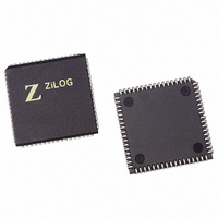
Z16C3516VSG Zilog, Z16C3516VSG Datasheet - Page 268

Z16C3516VSG
Manufacturer Part Number
Z16C3516VSG
Description
IC 16MHZ Z8500 CMOS ISCC 68-PLCC
Manufacturer
Zilog
Series
IUSC™r
Specifications of Z16C3516VSG
Controller Type
Serial Communications Controller (SCC)
Interface
USB
Voltage - Supply
4.75 V ~ 5.25 V
Current - Supply
50mA
Operating Temperature
0°C ~ 70°C
Mounting Type
Surface Mount
Package / Case
68-LCC (J-Lead)
Lead Free Status / RoHS Status
Lead free / RoHS Compliant
Other names
269-4690-5
Z16C3516VSG
Z16C3516VSG
Available stocks
Company
Part Number
Manufacturer
Quantity
Price
Company:
Part Number:
Z16C3516VSG
Manufacturer:
INTEL
Quantity:
6 219
- Current page: 268 of 268
- Download datasheet (3Mb)
Z16C35 ISCC™ User’s Manual
Zilog ISCC
Q. What’s the recovery time required for the ISCC?
A. A recovery time may apply to ANY access of the ISCC.
Q: Is the SDLC FIFO available in ISCC?
A: Yes, the SDLC FIFO is available in the SCC cell of the
18-2
ISCC QUESTIONS AND ANSWERS (Continued)
Thus, a bus transaction before or after an access of
the ISCC looks like it requires that the recovery time be
met for those accesses. The timing for /Strobe signals,
i.e. /DS, /WR, /RD or Pulsed /INTACK relative to CLK
is three clocks if /Strobe, synched to the /INTACK rel-
ative to CLK, is three clocks if /Strobe is synched to the
rising edge of CLK; or four clocks otherwise. The Re-
covery time is independent of /CS. Please note, if in
any design application with the ISCC the reads and
writes are unreliable, this recovery timing should be
checked very carefully and as this could be a bug with
the ISCC.
ISCC. There is a mistake in our ISCC Technical Man-
ual, P.5-20, on Register Description. The statement
'Bit 2 is not used and must be programmed “0”' is
wrong. Bit 2 of WR15 is used for enabling the SDLC
FIFO.
™
Controller
Q: Will DMA be enabled by writing the Enable
A: Yes, DMA operation is triggered by the command,
Q: Will DMA operation be triggered by the DMA en-
A: Yes, DMA operation will also be triggered by setting
Command in the Channel Command/Address Reg-
ister?
“Enable DMA” on Channel Command/Address Regis-
ter. This is another mistake in our ISCC Technical
Manual, P.5-25, on Registe Description. The state-
ment “DMA operation is not triggered by this com-
mand” is wrong, e.g., Writing “100” to bits 7 through 5
enables and triggers TxB DMA operation.
able command in the DMA Enable Register?
corresponding DMA Enable bits in the DMA Enable
Register (P.5-29 sec 5.6.7, DMA Enable Register in
ISCC Technical Manual). Note that this is a read/write
register. Read-modify-write instructions should be
used in writing this register to avoid the register value
to be overwritten and cause accidental enabling/dis-
abling of the DMA operations.
UM011001-0601
Related parts for Z16C3516VSG
Image
Part Number
Description
Manufacturer
Datasheet
Request
R

Part Number:
Description:
CMOS ISCC INTEGRATED SERIAL COMMUNICATIONS CONTROLLER
Manufacturer:
ZILOG [Zilog, Inc.]
Datasheet:

Part Number:
Description:
Communication Controllers, ZILOG INTELLIGENT PERIPHERAL CONTROLLER (ZIP)
Manufacturer:
Zilog, Inc.
Datasheet:

Part Number:
Description:
KIT DEV FOR Z8 ENCORE 16K TO 64K
Manufacturer:
Zilog
Datasheet:

Part Number:
Description:
KIT DEV Z8 ENCORE XP 28-PIN
Manufacturer:
Zilog
Datasheet:

Part Number:
Description:
DEV KIT FOR Z8 ENCORE 8K/4K
Manufacturer:
Zilog
Datasheet:

Part Number:
Description:
KIT DEV Z8 ENCORE XP 28-PIN
Manufacturer:
Zilog
Datasheet:

Part Number:
Description:
DEV KIT FOR Z8 ENCORE 4K TO 8K
Manufacturer:
Zilog
Datasheet:

Part Number:
Description:
CMOS Z8 microcontroller. ROM 16 Kbytes, RAM 256 bytes, speed 16 MHz, 32 lines I/O, 3.0V to 5.5V
Manufacturer:
Zilog, Inc.
Datasheet:

Part Number:
Description:
Low-cost microcontroller. 512 bytes ROM, 61 bytes RAM, 8 MHz
Manufacturer:
Zilog, Inc.
Datasheet:

Part Number:
Description:
Z8 4K OTP Microcontroller
Manufacturer:
Zilog, Inc.
Datasheet:

Part Number:
Description:
CMOS SUPER8 ROMLESS MCU
Manufacturer:
Zilog, Inc.
Datasheet:

Part Number:
Description:
SL1866 CMOSZ8 OTP Microcontroller
Manufacturer:
Zilog, Inc.
Datasheet:

Part Number:
Description:
SL1866 CMOSZ8 OTP Microcontroller
Manufacturer:
Zilog, Inc.
Datasheet:

Part Number:
Description:
OTP (KB) = 1, RAM = 125, Speed = 12, I/O = 14, 8-bit Timers = 2, Comm Interfaces Other Features = Por, LV Protect, Voltage = 4.5-5.5V
Manufacturer:
Zilog, Inc.
Datasheet:


