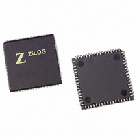
Z16C3516VSG Zilog, Z16C3516VSG Datasheet - Page 45

Z16C3516VSG
Manufacturer Part Number
Z16C3516VSG
Description
IC 16MHZ Z8500 CMOS ISCC 68-PLCC
Manufacturer
Zilog
Series
IUSC™r
Specifications of Z16C3516VSG
Controller Type
Serial Communications Controller (SCC)
Interface
USB
Voltage - Supply
4.75 V ~ 5.25 V
Current - Supply
50mA
Operating Temperature
0°C ~ 70°C
Mounting Type
Surface Mount
Package / Case
68-LCC (J-Lead)
Lead Free Status / RoHS Status
Lead free / RoHS Compliant
Other names
269-4690-5
Z16C3516VSG
Z16C3516VSG
Available stocks
Company
Part Number
Manufacturer
Quantity
Price
Company:
Part Number:
Z16C3516VSG
Manufacturer:
INTEL
Quantity:
6 219
- Current page: 45 of 268
- Download datasheet (3Mb)
UM011001-0601
For those applications requiring any other sync character
length, the ISCC makes provision for an external circuit to
provide a character synchronization signal on the /SYNC
pin. This mode is selected by setting bits D5 and D4 of
WR4 to “1”. In this mode the Sync/Hunt bit in RR0 reports
the state of the /SYNC pin but the receiver must still be
placed in Hunt mode when the external logic is searching
In all cases except External Sync mode the /SYNC pin is
an output that is driven Low by the ISCC to signal that a
sync character has been received. The /SYNC pin is
activated regardless of character boundaries so any
external circuitry using it should only respond the /SYNC
/SYNC
Sync7
Sync1
Sync7
Sync3
ADR7
ADR7
Sync7
Sync5
Sync15
Sync11
/RTxC
0
RxD
Sync6
Sync0
Sync6
Sync2
ADR6
ADR6
Sync6
Sync4
Sync14
Sync10
1
Write Register 6
Sync5
Sync5
Sync5
Sync1
ADR5
ADR5
D7
SYNC
Write Register 7
Sync5
Sync3
Sync13
Sync9
D7
1
D6
D6
Figure 4-5. Sync Character Programming
Last-
D5 D4 D3 D2 D1 D0
Sync4
Sync4
Sync4
Sync0
ADR4
ADR4
Sync4
Sync2
Sync12
Sync8
D5 D4 D3 D2 D1 D0
1
Figure 4-6. /SYNC as an Input
ADR3
Sync3
Sync3
Sync3
SYNC
Sync3
Sync1
Sync11
Sync7
x
1
1
ADR2
Sync2
Sync2
Sync2
Las
Sync2
Sync0
Sync10
Sync6
1
x
1
Sync1
Sync1
Sync1
ADR1
for a sync character match. When the receiver is in Hunt
mode and the /SYNC pin is driven Low, two receive clock
cycles after the last bit of the sync character is received,
character assembly will begin on the rising edge of the
receive clock immediately preceding the activation of
/SYNC. This is shown in Figure 4-6. The receiver leaves
Hunt mode when /SYNC is driven Low.
pulse that occurs while the receiver is in Hunt mode. The
timing for the /SYNC signal is shown in Figure 4-7.
Sync1
Sync9
Sync5
1
x
DATA
x
1
ADR0
Sync0
Sync0
Sync0
Sync0
Sync8
Sync4
1
x
0
x
0
Monosync, 8 Bits
Monosync, 6 Bits
Bisync, 16 Bits
Bisync, 12 Bits
SDLC
SDLC (Address Range)
Monosync, 8 Bits
Monosync, 6 Bits
Bisync, 16 Bits
Bisync, 12 Bits
SDLC
DATA
1
Z16C35ISCC™ User’s Manual
Data Communication Modes
DATA
2
4-11
4
Related parts for Z16C3516VSG
Image
Part Number
Description
Manufacturer
Datasheet
Request
R

Part Number:
Description:
CMOS ISCC INTEGRATED SERIAL COMMUNICATIONS CONTROLLER
Manufacturer:
ZILOG [Zilog, Inc.]
Datasheet:

Part Number:
Description:
Communication Controllers, ZILOG INTELLIGENT PERIPHERAL CONTROLLER (ZIP)
Manufacturer:
Zilog, Inc.
Datasheet:

Part Number:
Description:
KIT DEV FOR Z8 ENCORE 16K TO 64K
Manufacturer:
Zilog
Datasheet:

Part Number:
Description:
KIT DEV Z8 ENCORE XP 28-PIN
Manufacturer:
Zilog
Datasheet:

Part Number:
Description:
DEV KIT FOR Z8 ENCORE 8K/4K
Manufacturer:
Zilog
Datasheet:

Part Number:
Description:
KIT DEV Z8 ENCORE XP 28-PIN
Manufacturer:
Zilog
Datasheet:

Part Number:
Description:
DEV KIT FOR Z8 ENCORE 4K TO 8K
Manufacturer:
Zilog
Datasheet:

Part Number:
Description:
CMOS Z8 microcontroller. ROM 16 Kbytes, RAM 256 bytes, speed 16 MHz, 32 lines I/O, 3.0V to 5.5V
Manufacturer:
Zilog, Inc.
Datasheet:

Part Number:
Description:
Low-cost microcontroller. 512 bytes ROM, 61 bytes RAM, 8 MHz
Manufacturer:
Zilog, Inc.
Datasheet:

Part Number:
Description:
Z8 4K OTP Microcontroller
Manufacturer:
Zilog, Inc.
Datasheet:

Part Number:
Description:
CMOS SUPER8 ROMLESS MCU
Manufacturer:
Zilog, Inc.
Datasheet:

Part Number:
Description:
SL1866 CMOSZ8 OTP Microcontroller
Manufacturer:
Zilog, Inc.
Datasheet:

Part Number:
Description:
SL1866 CMOSZ8 OTP Microcontroller
Manufacturer:
Zilog, Inc.
Datasheet:

Part Number:
Description:
OTP (KB) = 1, RAM = 125, Speed = 12, I/O = 14, 8-bit Timers = 2, Comm Interfaces Other Features = Por, LV Protect, Voltage = 4.5-5.5V
Manufacturer:
Zilog, Inc.
Datasheet:


