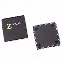
Z16C3516VSG Zilog, Z16C3516VSG Datasheet - Page 134

Z16C3516VSG
Manufacturer Part Number
Z16C3516VSG
Description
IC 16MHZ Z8500 CMOS ISCC 68-PLCC
Manufacturer
Zilog
Series
IUSC™r
Specifications of Z16C3516VSG
Controller Type
Serial Communications Controller (SCC)
Interface
USB
Voltage - Supply
4.75 V ~ 5.25 V
Current - Supply
50mA
Operating Temperature
0°C ~ 70°C
Mounting Type
Surface Mount
Package / Case
68-LCC (J-Lead)
Lead Free Status / RoHS Status
Lead free / RoHS Compliant
Other names
269-4690-5
Z16C3516VSG
Z16C3516VSG
Available stocks
Company
Part Number
Manufacturer
Quantity
Price
Company:
Part Number:
Z16C3516VSG
Manufacturer:
INTEL
Quantity:
6 219
- Current page: 134 of 268
- Download datasheet (3Mb)
Application Note
The Z180™ Interfaced with the SCC at MHZ
INPUT/OUTPUT CYCLES
Although the SCC is a universal design, certain timing
parameters differ from the Z180 timing. The following
subsections discuss the I/O interface for the Z180 MPU
and SCC.
SCC I/O Read/Write Cycle
Assume that the Z180 MPU’s /IOC bit in the OMCR
(Operation Mode Control Register) clears to 0 (this
condition is a Z80 compatible timing mode for /IORQ and
/RD). The following are several design points to consider
(also see Table 3).
I/O Read Cycle
Parameters 8 and 9 mean that Address is stable 20 ns
before the falling edge of /RD and until /RD goes inactive.
Parameters 19 and 20 mean that /CE is stable at the falling
edge of /RD and until /RD goes inactive.
Parameter 22 means the /RD pulse width is wider than
125 ns.
Parameters 25 and 27 mean that Read data is available on
the data bus 120 ns later than the falling edge of /RD and
180 ns from a stable Address.
7-14
No
6
7
8
9
16
17
19
20
22
25
27
28
29
30
Symbol
TsA(WR)
ThA(WR)
TsA(RD)
ThA(RD)
TsCEI(WR)
ThCE(WR)
TsCEI(RD)
ThCE(RD)
TwRDI
TdRDf(DR)
TdA(DR)
TwWRI
TsDW(WR)
TdWR(W)
Table 7. 10 MHz SCC Timing Parameters for I/O Read/Write Cycle (Worst Case)
Parameter
Address to /WR Low Setup
Address to /WR High Hold
Address to /RD Low Setup
Address to /RD High Hold
/CE Low to /WR Low Setup
/CE to /WR High Hold
/CE Low to /RD Low Setup
/CE to /RD High Hold
/RD Low Width
/RD Low to Read Data Valid
Address to Read Data Valid
/WR Low Width
Write Data to /WR Low Setup
Write Data to /WR High Hold
Z180 MPU to SCC Interface
Table 7 shows key parameters of the 10 MHz SCC for I/O
read/write cycles.
I/O Write Cycle
Parameters 6 and 7 mean that Address is stable 50 ns
before the falling edge of /WR and is stable until /WR goes
inactive.
Parameters 16 and 17 mean that /CE is stable at the falling
edge of /WR and is stable until /W goes inactive.
Parameter 28 means /WR pulse width is wider than 125
ns.
Parameters 28 and 29 mean that Write data is on the data
bus 10 ns before the falling edge of /WR. It is stable until
the rising edge of /WR.
Tables 8 and 9 show the worst case SCC parameters
calculating Z180 parameters at 10 MHz.
Min
125
125
50
50
10
0
0
0
0
0
0
0
Max
120
180
UM011001-0601
Units
ns
ns
ns
ns
ns
ns
ns
ns
ns
ns
ns
ns
ns
ns
Related parts for Z16C3516VSG
Image
Part Number
Description
Manufacturer
Datasheet
Request
R

Part Number:
Description:
CMOS ISCC INTEGRATED SERIAL COMMUNICATIONS CONTROLLER
Manufacturer:
ZILOG [Zilog, Inc.]
Datasheet:

Part Number:
Description:
Communication Controllers, ZILOG INTELLIGENT PERIPHERAL CONTROLLER (ZIP)
Manufacturer:
Zilog, Inc.
Datasheet:

Part Number:
Description:
KIT DEV FOR Z8 ENCORE 16K TO 64K
Manufacturer:
Zilog
Datasheet:

Part Number:
Description:
KIT DEV Z8 ENCORE XP 28-PIN
Manufacturer:
Zilog
Datasheet:

Part Number:
Description:
DEV KIT FOR Z8 ENCORE 8K/4K
Manufacturer:
Zilog
Datasheet:

Part Number:
Description:
KIT DEV Z8 ENCORE XP 28-PIN
Manufacturer:
Zilog
Datasheet:

Part Number:
Description:
DEV KIT FOR Z8 ENCORE 4K TO 8K
Manufacturer:
Zilog
Datasheet:

Part Number:
Description:
CMOS Z8 microcontroller. ROM 16 Kbytes, RAM 256 bytes, speed 16 MHz, 32 lines I/O, 3.0V to 5.5V
Manufacturer:
Zilog, Inc.
Datasheet:

Part Number:
Description:
Low-cost microcontroller. 512 bytes ROM, 61 bytes RAM, 8 MHz
Manufacturer:
Zilog, Inc.
Datasheet:

Part Number:
Description:
Z8 4K OTP Microcontroller
Manufacturer:
Zilog, Inc.
Datasheet:

Part Number:
Description:
CMOS SUPER8 ROMLESS MCU
Manufacturer:
Zilog, Inc.
Datasheet:

Part Number:
Description:
SL1866 CMOSZ8 OTP Microcontroller
Manufacturer:
Zilog, Inc.
Datasheet:

Part Number:
Description:
SL1866 CMOSZ8 OTP Microcontroller
Manufacturer:
Zilog, Inc.
Datasheet:

Part Number:
Description:
OTP (KB) = 1, RAM = 125, Speed = 12, I/O = 14, 8-bit Timers = 2, Comm Interfaces Other Features = Por, LV Protect, Voltage = 4.5-5.5V
Manufacturer:
Zilog, Inc.
Datasheet:


