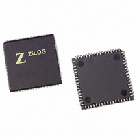
Z16C3516VSG Zilog, Z16C3516VSG Datasheet - Page 48

Z16C3516VSG
Manufacturer Part Number
Z16C3516VSG
Description
IC 16MHZ Z8500 CMOS ISCC 68-PLCC
Manufacturer
Zilog
Series
IUSC™r
Specifications of Z16C3516VSG
Controller Type
Serial Communications Controller (SCC)
Interface
USB
Voltage - Supply
4.75 V ~ 5.25 V
Current - Supply
50mA
Operating Temperature
0°C ~ 70°C
Mounting Type
Surface Mount
Package / Case
68-LCC (J-Lead)
Lead Free Status / RoHS Status
Lead free / RoHS Compliant
Other names
269-4690-5
Z16C3516VSG
Z16C3516VSG
Available stocks
Company
Part Number
Manufacturer
Quantity
Price
Company:
Part Number:
Z16C3516VSG
Manufacturer:
INTEL
Quantity:
6 219
- Current page: 48 of 268
- Download datasheet (3Mb)
Z16C35ISCC™ User’s Manual
Data Communication Modes
4.3 BYTE-ORIENTED SYNCHRONOUS MODE (Continued)
3. Character C is loaded into the receive data FIFO and
4. Now E is loaded into the receive data FIFO. During the
4-14
processor reads B and enables CRC. At the end of this
eight-bit time, B is in the 8-bit delay and C is in the
receive shift register.
at the same time the CRC checker becomes enabled.
During the next eight-bit-time, the processor reads C
and since CRC is enabled within this period, the ISCC
has calculated CRC on character B; character C is in
the 8-bit delay and D is in the Receive Shift register. D
is then loaded into the receive data FIFO and at some
point during the next eight-bit-time the processor
reads D and disables CRC. At the end of these eight-
bit-times CRC has been calculated on C, character D
is in the 8-bit delay and E is in the Receive Shift
register.
next eight-bit-times the processor reads E and
enables the CRC. During this time E shifts into the 8-
bit delay, F enters the Receive Shift register and CRC
is not being calculated on D. After these eight-bit-times
have elapsed, E is in the 8-bit delay, and F is in the
Receive Shift register. Now F is transferred to the
receive data FIFO and CRC is enabled. During the
next eight-bit-times the processor reads F and leaves
the CRC enabled. The processor is usually aware that
this is the last character in the message and so
prepares to check the result of the CRC computation.
However, another sixteen bit-times are required
before CRC has been calculated on all of character F.
5. At the end of eight-bit-times F is in the 8-bit delay and
Receive Data
G is in the Receive Shift register. At this time G is
transferred to the receive data FIFO. Character G
must be read and discarded by the processor. Eight bit
times later H is transferred to the receive data FIFO
also. The result of a CRC calculation is latched in the
receive error FIFO at the same time as data is written
to the receive data FIFO. Thus the CRC result through
character F accompanies character H in the FIFO and
will be valid in RR1 until character H is read from the
receive data FIFO. The CRC checker may be disabled
and reset at any time after character H is transferred
to the receive data FIFO. Recall, however, that
internally CRC will not be disabled until after this
occurs. A better alternative is to place the receiver in
Hunt mode, which automatically disables and resets
the CRC checker. See Table 4-8 for a condensed
description.
Figure 4-9. Receive CRC Data Path
Receive Shift Register
Eight Bit Time Delay
Receive Data FIFO
CRC Checker
UM011001-0601
Related parts for Z16C3516VSG
Image
Part Number
Description
Manufacturer
Datasheet
Request
R

Part Number:
Description:
CMOS ISCC INTEGRATED SERIAL COMMUNICATIONS CONTROLLER
Manufacturer:
ZILOG [Zilog, Inc.]
Datasheet:

Part Number:
Description:
Communication Controllers, ZILOG INTELLIGENT PERIPHERAL CONTROLLER (ZIP)
Manufacturer:
Zilog, Inc.
Datasheet:

Part Number:
Description:
KIT DEV FOR Z8 ENCORE 16K TO 64K
Manufacturer:
Zilog
Datasheet:

Part Number:
Description:
KIT DEV Z8 ENCORE XP 28-PIN
Manufacturer:
Zilog
Datasheet:

Part Number:
Description:
DEV KIT FOR Z8 ENCORE 8K/4K
Manufacturer:
Zilog
Datasheet:

Part Number:
Description:
KIT DEV Z8 ENCORE XP 28-PIN
Manufacturer:
Zilog
Datasheet:

Part Number:
Description:
DEV KIT FOR Z8 ENCORE 4K TO 8K
Manufacturer:
Zilog
Datasheet:

Part Number:
Description:
CMOS Z8 microcontroller. ROM 16 Kbytes, RAM 256 bytes, speed 16 MHz, 32 lines I/O, 3.0V to 5.5V
Manufacturer:
Zilog, Inc.
Datasheet:

Part Number:
Description:
Low-cost microcontroller. 512 bytes ROM, 61 bytes RAM, 8 MHz
Manufacturer:
Zilog, Inc.
Datasheet:

Part Number:
Description:
Z8 4K OTP Microcontroller
Manufacturer:
Zilog, Inc.
Datasheet:

Part Number:
Description:
CMOS SUPER8 ROMLESS MCU
Manufacturer:
Zilog, Inc.
Datasheet:

Part Number:
Description:
SL1866 CMOSZ8 OTP Microcontroller
Manufacturer:
Zilog, Inc.
Datasheet:

Part Number:
Description:
SL1866 CMOSZ8 OTP Microcontroller
Manufacturer:
Zilog, Inc.
Datasheet:

Part Number:
Description:
OTP (KB) = 1, RAM = 125, Speed = 12, I/O = 14, 8-bit Timers = 2, Comm Interfaces Other Features = Por, LV Protect, Voltage = 4.5-5.5V
Manufacturer:
Zilog, Inc.
Datasheet:


