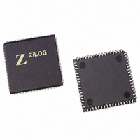
Z16C3516VSG Zilog, Z16C3516VSG Datasheet - Page 54

Z16C3516VSG
Manufacturer Part Number
Z16C3516VSG
Description
IC 16MHZ Z8500 CMOS ISCC 68-PLCC
Manufacturer
Zilog
Series
IUSC™r
Specifications of Z16C3516VSG
Controller Type
Serial Communications Controller (SCC)
Interface
USB
Voltage - Supply
4.75 V ~ 5.25 V
Current - Supply
50mA
Operating Temperature
0°C ~ 70°C
Mounting Type
Surface Mount
Package / Case
68-LCC (J-Lead)
Lead Free Status / RoHS Status
Lead free / RoHS Compliant
Other names
269-4690-5
Z16C3516VSG
Z16C3516VSG
Available stocks
Company
Part Number
Manufacturer
Quantity
Price
Company:
Part Number:
Z16C3516VSG
Manufacturer:
INTEL
Quantity:
6 219
- Current page: 54 of 268
- Download datasheet (3Mb)
Z16C35ISCC™ User’s Manual
Data Communication Modes
4.4 BIT-ORIENTED SYNCHRONOUS MODE (Continued)
4.4.2 SDLC Receive
The receiver in the ISCC™ always searches the receive
data stream for flag characters in SDLC mode. Ordinarily,
the receiver transfers all received data between flags to
the receive data FIFO. However, if the receiver is in Hunt
mode no flag is received. The receiver is in Hunt mode
when first enabled, or the receiver may be placed in Hunt
mode by the processor issuing the Enter Hunt mode com-
mand in WR3. this bit (D4) is a command, and writing a “0”
to it has no effect. The Hunt status of the receiver is report-
ed by the Sync/Hunt bit in RR0.
Sync/Hunt is one of the possible sources of external/status
interrupts, with both transitions causing an interrupt. This
If the Address Search Mode bit (D2) in WR3 is set to “0”
the address recognition logic is disabled and all received
frames are transferred to the receive data FIFO. In this
mode the software must perform any address recognition.
If the Address Search Mode bit is set to “1”, only those
frames whose address matches the address programmed
in WR6 or the global address (all “1s”) will be transferred
to the receive data FIFO.
The address comparison will be across all eight bits of
WR6 if the Sync Character Load inhibit bit (D1) in WR3 is
set to “0”. The comparison may be modified so that only
the four most significant bits of WR6 must match the re-
ceived address. This mode is selected by setting the Sync
Character Load inhibit bit to “1”. In this mode, however, the
address field is still eight bits wide. The address field is
transferred to the receive data FIFO in the same manner
as data. It is not treated differently than data.
4-20
/SYNC
/RTxC
PCLK
Figure 4-12. /SYNC as an Output
is true even if the Sync/Hunt bit is set as a result of the pro-
cessor issuing the Enter Hunt mode command.
The receiver will automatically enter Hunt mode if an abort
is received. Because the receiver always searches the re-
ceive data stream for flags and automatically enters Hunt
Mode when an abort is received, the receiver will always
handle frames correctly, and the Enter Hunt Mode com-
mand should never be needed. The ISCC will drive the
SYNC pin Low to signal that a flag has been recognized.
The timing for the SYNC signal is shown in Figure 4-12.
The first byte in an SDLC frame is assumed by the ISCC
to be the address of the secondary station for which the
frame is intended. The ISCC provides several options for
handling this address.
The number of bits per character is controlled by bits D7
and D6 of WR3. Five, six, seven, or eight bits per character
may be selected via these two bits. The data is right-justi-
fied in the receive buffer. The ISCC merely takes a snap-
shot of the receive data stream at the appropriate times, so
the “unused” receive buffer are only the bits following the
character.
An additional bit carrying parity information may be selected
by setting bit D6 of WR4 to “1”. This also enables parity in
the transmitter. The parity sense is selected by bit D1 of
WR4. Parity is not normally used in SDLC mode. The
character length may be changed at any time before the
new number of bits have been assembled by the receiver.
Care should be exercised, however, as unexpected results
may occur. A representative example, switching from five
bits to eight bits and back to five bits is shown in Figure 4-13.
State changes in one
/RTxC clock cycle
UM011001-0601
Related parts for Z16C3516VSG
Image
Part Number
Description
Manufacturer
Datasheet
Request
R

Part Number:
Description:
CMOS ISCC INTEGRATED SERIAL COMMUNICATIONS CONTROLLER
Manufacturer:
ZILOG [Zilog, Inc.]
Datasheet:

Part Number:
Description:
Communication Controllers, ZILOG INTELLIGENT PERIPHERAL CONTROLLER (ZIP)
Manufacturer:
Zilog, Inc.
Datasheet:

Part Number:
Description:
KIT DEV FOR Z8 ENCORE 16K TO 64K
Manufacturer:
Zilog
Datasheet:

Part Number:
Description:
KIT DEV Z8 ENCORE XP 28-PIN
Manufacturer:
Zilog
Datasheet:

Part Number:
Description:
DEV KIT FOR Z8 ENCORE 8K/4K
Manufacturer:
Zilog
Datasheet:

Part Number:
Description:
KIT DEV Z8 ENCORE XP 28-PIN
Manufacturer:
Zilog
Datasheet:

Part Number:
Description:
DEV KIT FOR Z8 ENCORE 4K TO 8K
Manufacturer:
Zilog
Datasheet:

Part Number:
Description:
CMOS Z8 microcontroller. ROM 16 Kbytes, RAM 256 bytes, speed 16 MHz, 32 lines I/O, 3.0V to 5.5V
Manufacturer:
Zilog, Inc.
Datasheet:

Part Number:
Description:
Low-cost microcontroller. 512 bytes ROM, 61 bytes RAM, 8 MHz
Manufacturer:
Zilog, Inc.
Datasheet:

Part Number:
Description:
Z8 4K OTP Microcontroller
Manufacturer:
Zilog, Inc.
Datasheet:

Part Number:
Description:
CMOS SUPER8 ROMLESS MCU
Manufacturer:
Zilog, Inc.
Datasheet:

Part Number:
Description:
SL1866 CMOSZ8 OTP Microcontroller
Manufacturer:
Zilog, Inc.
Datasheet:

Part Number:
Description:
SL1866 CMOSZ8 OTP Microcontroller
Manufacturer:
Zilog, Inc.
Datasheet:

Part Number:
Description:
OTP (KB) = 1, RAM = 125, Speed = 12, I/O = 14, 8-bit Timers = 2, Comm Interfaces Other Features = Por, LV Protect, Voltage = 4.5-5.5V
Manufacturer:
Zilog, Inc.
Datasheet:


