LPC47B272-MS SMSC, LPC47B272-MS Datasheet - Page 59
LPC47B272-MS
Manufacturer Part Number
LPC47B272-MS
Description
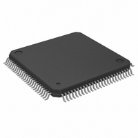
IC CTRLR SUPER I/O LPC 100-QFP
Manufacturer
SMSC
Datasheet
1.LPC47B272-MS.pdf
(195 pages)
Specifications of LPC47B272-MS
Controller Type
I/O Controller
Interface
LPC
Voltage - Supply
3.3V
Current - Supply
15mA
Operating Temperature
0°C ~ 70°C
Mounting Type
Surface Mount
Package / Case
100-QFP
Lead Free Status / RoHS Status
Lead free / RoHS Compliant
Other names
638-1019
Available stocks
Company
Part Number
Manufacturer
Quantity
Price
Company:

Part Number:
LPC47B272-MS
Manufacturer:
ADI
Quantity:
957
Company:
Part Number:
LPC47B272-MS
Manufacturer:
Microchip Technology
Quantity:
10 000
Part Number:
LPC47B272-MS
Manufacturer:
SMSC
Quantity:
20 000


Bit 4
Even Parity Select bit. When bit 3 is a logic "1" and bit 4 is a logic "0", an odd number of logic "1"'s is transmitted or
checked in the data word bits and the parity bit. When bit 3 is a logic "1" and bit 4 is a logic "1" an even number of bits is
transmitted and checked.
Bit 5
Stick Parity bit. When parity is enabled it is used in conjunction with bit 4 to select Mark or Space Parity. When LCR bits
3, 4 and 5 are 1 the Parity bit is transmitted and checked as a 0 (Space Parity). If bits 3 and 5 are 1 and bit 4 is a 0, then
the Parity bit is transmitted and checked as 1 (Mark Parity). If bit 5 is 0 Stick Parity is disabled.
Bit 6
Set Break Control bit. When bit 6 is a logic "1", the transmit data output (TXD) is forced to the Spacing or logic "0" state
and remains there (until reset by a low level bit 6) regardless of other transmitter activity. This feature enables the Serial
Port to alert a terminal in a communications system.
Bit 7
Divisor Latch Access bit (DLAB). It must be set high (logic "1") to access the Divisor Latches of the Baud Rate
Generator during read or write operations. It must be set low (logic "0") to access the Receiver Buffer Register, the
Transmitter Holding Register, or the Interrupt Enable Register.
MODEM CONTROL REGISTER (MCR)
Address Offset = 4H, DLAB = X, READ/WRITE
This 8 bit register controls the interface with the MODEM or data set (or device emulating a MODEM). The contents of
the MODEM control register are described below.
Bit 0
This bit controls the Data Terminal Ready (nDTR) output. When bit 0 is set to a logic "1", the nDTR output is forced to a
logic "0". When bit 0 is a logic "0", the nDTR output is forced to a logic "1".
Bit 1
This bit controls the Request To Send (nRTS) output. Bit 1 affects the nRTS output in a manner identical to that
described above for bit 0.
Bit 2
This bit controls the Output 1 (OUT1) bit. This bit does not have an output pin and can only be read or written by the
CPU.
Bit 3
Output 2 (OUT2). This bit is used to enable an UART interrupt. When OUT2 is a logic "0", the serial port interrupt
output is forced to a high impedance state - disabled. When OUT2 is a logic "1", the serial port interrupt outputs are
enabled.
Bit 4
This bit provides the loopback feature for diagnostic testing of the Serial Port. When bit 4 is set to logic "1", the following
occur:
1. The TXD is set to the Marking State(logic "1").
2. The receiver Serial Input (RXD) is disconnected.
3. The output of the Transmitter Shift Register is "looped back" into the Receiver Shift Register input.
4. All MODEM Control inputs (nCTS, nDSR, nRI and nDCD) are disconnected.
5. The four MODEM Control outputs (nDTR, nRTS, OUT1 and OUT2) are internally connected to the four MODEM
Control inputs (nDSR, nCTS, RI, DCD).
6.
The Modem Control output pins are forced inactive high.
7. Data that is transmitted is immediately received.
This feature allows the processor to verify the transmit and receive data paths of the Serial Port. In the diagnostic mode,
the receiver and the transmitter interrupts are fully operational. The MODEM Control Interrupts are also operational but
the interrupts' sources are now the lower four bits of the MODEM Control Register instead of the MODEM Control
inputs. The interrupts are still controlled by the Interrupt Enable Register.
Bits 5 through 7
These bits are permanently set to logic zero.
SMSC LPC47B27x
- 59 -
Rev. 04-17-07
DATASHEET
Related parts for LPC47B272-MS
Image
Part Number
Description
Manufacturer
Datasheet
Request
R


Part Number:
Description:
FAST ETHERNET PHYSICAL LAYER DEVICE
Manufacturer:
SMSC Corporation
Datasheet:
Part Number:
Description:
357-036-542-201 CARDEDGE 36POS DL .156 BLK LOPRO
Manufacturer:
SMSC Corporation
Datasheet:
Part Number:
Description:
357-036-542-201 CARDEDGE 36POS DL .156 BLK LOPRO
Manufacturer:
SMSC Corporation
Datasheet:
Part Number:
Description:
357-036-542-201 CARDEDGE 36POS DL .156 BLK LOPRO
Manufacturer:
SMSC Corporation
Datasheet:
Part Number:
Description:
4-PORT USB2.0 HUB CONTROLLER
Manufacturer:
SMSC Corporation
Datasheet:
Part Number:
Description:
Manufacturer:
SMSC Corporation
Datasheet:
Part Number:
Description:
Manufacturer:
SMSC Corporation
Datasheet:
Part Number:
Description:
FDC37C672ENHANCED SUPER I/O CONTROLLER WITH FAST IR
Manufacturer:
SMSC Corporation
Datasheet:
Part Number:
Description:
COM90C66LJPARCNET Controller/Transceiver with AT Interface and On-Chip RAM
Manufacturer:
SMSC Corporation
Datasheet:
Part Number:
Description:
Manufacturer:
SMSC Corporation
Datasheet:
Part Number:
Description:
Manufacturer:
SMSC Corporation
Datasheet:
Part Number:
Description:
Manufacturer:
SMSC Corporation
Datasheet:
Part Number:
Description:
Manufacturer:
SMSC Corporation
Datasheet: