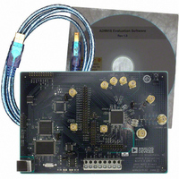
AD9910/PCBZ Analog Devices Inc, AD9910/PCBZ Datasheet - Page 60

AD9910/PCBZ
Manufacturer Part Number
AD9910/PCBZ
Description
Direct Digital Synthesis Evaluation Board
Manufacturer
Analog Devices Inc
Series
AgileRF™r
Specifications of AD9910/PCBZ
Silicon Manufacturer
Analog Devices
Application Sub Type
Direct Digital Synthesizer
Kit Application Type
Clock & Timing
Silicon Core Number
AD9910
Kit Contents
Board
Design Resources
Synchronizing Multiple AD9910 1 GSPS Direct Digital Synthesizers (CN0121)
Main Purpose
Timing, Direct Digital Synthesis (DDS)
Embedded
No
Utilized Ic / Part
AD9910
Primary Attributes
14-Bit DAC, 32-Bit Tuning Word Width
Secondary Attributes
1GHz, Graphical User Interface
Lead Free Status / RoHS Status
Lead free / RoHS Compliant
Lead Free Status / RoHS Status
Lead free / RoHS Compliant, Lead free / RoHS Compliant
Other names
Q3335404
AD9910
Multichip Sync Register—Address 0x0A
Four bytes are assigned to this register.
Table 26. Multichip Sync Register
Bit(s)
31:28
27
26
25
24
23:18
17:16
15:11
10:8
7:3
2:0
Digital Ramp Limit Register—Address 0x0B
Eight bytes are assigned to this register. This register is only effective if CFR2[19] = 1. See the Digital Ramp Generator (DRG) section for
details.
Table 27. Bit Descriptions for Digital Ramp Limit Register
Bit(s)
63:32
31:0
Digital Ramp Step Size Register—Address 0x0C
Eight bytes are assigned to this register. This register is only effective if CFR2[19] = 1. See the Digital Ramp Generator (DRG) section for
details.
Table 28. Bit Descriptions for Digital Ramp Step Size Register
Bit(s)
63:32
31:0
Digital Ramp Rate Register—Address 0x0D
Four bytes are assigned to this register. This register is only effective if CFR2[19] = 1. See the Digital Ramp Generator (DRG) section for
details.
Table 29. Bit Descriptions for Digital Ramp Rate Register
Bit(s)
31:16
15:0
Mnemonic
Digital ramp upper limit
Digital ramp lower limit
Mnemonic
Digital ramp decrement
step size
Digital ramp increment
step size
Mnemonic
Digital ramp negative slope
rate
Digital ramp positive slope
rate
Mnemonic
Sync validation delay
Sync receiver enable
Sync generator enable
Sync generator polarity
Open
Sync state preset value
Open
Output sync generator
delay
Open
Input sync receiver delay
Open
Description
This 4-bit number sets the timing skew (in ~150 ps increments) between SYSCLK and the
delayed SYNC_INx signal for the sync validation block in the sync receiver. Default is 0000b.
0 = synchronization clock receiver disabled (default).
1 = synchronization clock receiver enabled.
0 = synchronization clock generator disabled (default).
1 = synchronization clock generator enabled.
0 = synchronization clock generator coincident with the rising edge of SYSCLK (default).
1 = synchronization clock generator coincident with the falling edge of SYSCLK.
This 6-bit number is the state that the internal clock generator assumes when it receives a
sync pulse. Default is 000000b.
This 5-bit number sets the output delay (in ~150 ps increments) of the sync generator.
Default is 00000b.
This 5-bit number sets the input delay (in ~150 ps increments) of the sync receiver. Default
is 00000b.
Description
32-bit digital ramp upper limit value.
32-bit digital ramp lower limit value.
Description
32-bit digital ramp decrement step size value.
32-bit digital ramp increment step size value.
Description
16-bit digital ramp negative slope value that defines the time interval between decrement
values.
16-bit digital ramp positive slope value that defines the time interval between increment
values.
Rev. C | Page 60 of 64


