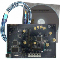
AD9910/PCBZ Analog Devices Inc, AD9910/PCBZ Datasheet - Page 30

AD9910/PCBZ
Manufacturer Part Number
AD9910/PCBZ
Description
Direct Digital Synthesis Evaluation Board
Manufacturer
Analog Devices Inc
Series
AgileRF™r
Specifications of AD9910/PCBZ
Silicon Manufacturer
Analog Devices
Application Sub Type
Direct Digital Synthesizer
Kit Application Type
Clock & Timing
Silicon Core Number
AD9910
Kit Contents
Board
Design Resources
Synchronizing Multiple AD9910 1 GSPS Direct Digital Synthesizers (CN0121)
Main Purpose
Timing, Direct Digital Synthesis (DDS)
Embedded
No
Utilized Ic / Part
AD9910
Primary Attributes
14-Bit DAC, 32-Bit Tuning Word Width
Secondary Attributes
1GHz, Graphical User Interface
Lead Free Status / RoHS Status
Lead free / RoHS Compliant
Lead Free Status / RoHS Status
Lead free / RoHS Compliant, Lead free / RoHS Compliant
Other names
Q3335404
AD9910
DRG Slope Control
The core of the DRG is a 32-bit accumulator clocked by a
programmable timer. The time base for the timer is the DDS
clock, which operates at ¼ f
interval between successive updates of the accumulator. The
positive (+Δt) and negative (−Δt) slope step intervals are
independently programmable as given by
where P and N are the two 16-bit values stored in the 32-bit digital
ramp rate register and control the step interval. N defines the step
interval of the negative slope portion of the ramp. P defines the step
interval of the positive slope portion of the ramp.
The step size of the positive (STEP
portions of the ramp are 32-bit values programmed into the 64-bit
digital ramp step size register. Program each of the step sizes as an
unsigned integer (the hardware automatically interprets STEP
a negative value). The relationship between the 32-bit step size
values and actual units of frequency, phase, or amplitude depend
on the digital ramp destination bits. Calculate the actual frequency,
phase, or amplitude step size by substituting STEP
for M in the following equations as required:
Note that the frequency units are the same as those used to
represent f
the same as those used to represent I
current of the DAC (mA, for example).
The phase and amplitude step size equations yield the average
step size. Although the step size accumulates with 32-bit precision,
the phase or amplitude destination exhibits only 16 or 14 bits,
respectively. Therefore, at the destination, the actual phase or
amplitude step is the accumulated 32-bit value truncated to 16
or 14 bits, respectively.
+
−
Frequency
Phase
Phase
Amplitude
Δ =
Δ =
t
t
SYSCLK
Step
Step
f
f
SYSCLK
SYSCLK
4
4
N
P
Step
=
=
Step
(MHz, for example). The amplitude units are
π
45M
2
2
M
31
=
29
=
⎛
⎜
⎝
⎛
⎜
⎝
2
M
2
M
32
32
⎞
⎟
⎠
SYSCLK
⎞
⎟
⎠
f
I
SYSCLK
FS
. The timer establishes the
P
) and negative (STEP
FS
, the full-scale output
N
or STEP
N
) slope
(radians)
(degrees)
N
P
as
Rev. C | Page 30 of 64
As described previously, the step interval is controlled by a
16-bit programmable timer. There are three events that can
cause this timer to be reloaded prior to its expiration. One event
occurs when the digital ramp enable bit transitions from cleared
to set, followed by an I/O update. A second event is a change of
state in the DRCTL pin. The third event is enabled using the load
LRR @ I/O update bit (see the Register Map and Bit Descriptions
section for details).
DRG Limit Control
The ramp accumulator is followed by limit control logic that
enforces an upper and lower boundary on the output of the
ramp generator. Under no circumstances does the output of the
DRG exceed the programmed limit values while the DRG is
enabled. The limits are set through the 64-bit digital ramp limit
register. Note that the upper limit value must be greater than the
lower limit value to ensure normal operation.
DRG Accumulator Clear
The ramp accumulator can be cleared (that is, reset to 0) under
program control. When the ramp accumulator is cleared, it forces
the DRG output to the lower limit programmed into the digital
ramp limit register.
With the limit control block embedded in the feedback path of the
accumulator, resetting the accumulator is equivalent to presetting it
to the lower limit value.
Normal Ramp Generation
Normal ramp generation implies that both no-dwell bits are
cleared (see the No-Dwell Ramp Generation section for details).
In Figure 39, a sample ramp waveform is depicted with the
required control signals. The top trace is the DRG output.
The next trace down is the status of the DROVER output pin
(assuming that the DROVER pin active bit is set). The remaining
traces are control bits and control pins. The pertinent ramp
parameters are also identified (upper and lower limits plus step
size and Δt for the positive and negative slopes). Along the
bottom, circled numbers identify specific events. These events
are referred to by number (Event 1 and so on) in the following
paragraphs.
In this particular example, the positive and negative slopes of
the ramp are different to demonstrate the flexibility of the DRG.
The parameters of both slopes can be programmed to make the
positive and negative slopes the same.


