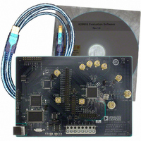
AD9910/PCBZ Analog Devices Inc, AD9910/PCBZ Datasheet - Page 31

AD9910/PCBZ
Manufacturer Part Number
AD9910/PCBZ
Description
Direct Digital Synthesis Evaluation Board
Manufacturer
Analog Devices Inc
Series
AgileRF™r
Specifications of AD9910/PCBZ
Silicon Manufacturer
Analog Devices
Application Sub Type
Direct Digital Synthesizer
Kit Application Type
Clock & Timing
Silicon Core Number
AD9910
Kit Contents
Board
Design Resources
Synchronizing Multiple AD9910 1 GSPS Direct Digital Synthesizers (CN0121)
Main Purpose
Timing, Direct Digital Synthesis (DDS)
Embedded
No
Utilized Ic / Part
AD9910
Primary Attributes
14-Bit DAC, 32-Bit Tuning Word Width
Secondary Attributes
1GHz, Graphical User Interface
Lead Free Status / RoHS Status
Lead free / RoHS Compliant
Lead Free Status / RoHS Status
Lead free / RoHS Compliant, Lead free / RoHS Compliant
Other names
Q3335404
Event 1—The digital ramp enable bit is set, which has no effect
on the DRG output because the bit is not effective until an I/O
update.
Event 2—An I/O update registers the enable bit. If DRCTL = 1
is in effect at this time (the gray portion of the DRCTL trace),
then the DRG output immediately begins a positive slope (the
gray portion of the DRG output trace). Otherwise, if DRCTL =
0, the DRG output is initialized to the lower limit.
Event 3—DRCTL transitions to a Logic 1 to initiate a positive
slope at the DRG output. In this example, the DRCTL pin is
held long enough to cause the DRG to reach its programmed
upper limit. The DRG remains at the upper limit until the ramp
accumulator is cleared, DRCTL = 0, or the upper limit is
reprogrammed to a higher value. In the last case, the DRG
immediately resumes its previous positive slope profile.
Event 4—DRCTL transitions to a Logic 0 to initiate a negative
slope at the DRG output. In this example, the DRCTL pin is
held long enough to cause the DRG to reach its programmed
lower limit. The DRG remains at the lower limit until DRCTL = 1,
or until the lower limit is reprogrammed to a lower value. In the
latter case, the DRG immediately resumes its previous negative
slope profile.
Event 5—DRCTL transitions to a Logic 1 for the second time,
initiating a second positive slope.
Event 6—The positive slope profile is interrupted by DRHOLD
transitioning to a Logic 1. This stalls the ramp accumulator and
freezes the DRG output at its last value.
DIGITAL RAMP ENABLE
RAMP ACCUMULATOR
RAMP ACCUMULATOR
AUTOCLEAR DIGITAL
CLEAR DIGITAL
DRG OUTPUT
I/O_UPDATE
DROVER
DRHOLD
DRCTL
1
2
P DDS CLOCK CYCLES
3
+Δ
t
LOWER LIMIT
Figure 39. Normal Ramp Generation
STEP SIZE
POSITIVE
N DDS CLOCK CYCLES
Rev. C | Page 31 of 64
4
–Δ
Event 7—DRHOLD transitions to a Logic 0, releasing the ramp
accumulator and reinstating the previous positive slope profile.
Event 8—The clear digital ramp accumulator bit is set, which
has no effect on the DRG because the bit is not effective until an
I/O update is issued.
Event 9—An I/O update registers that the clear digital ramp
accumulator bit is set, resetting the ramp accumulator and
forcing the DRG output to the programmed lower limit. The
DRG output remains at the lower limit until the clear condition
is removed.
Event 10—The clear digital ramp accumulator bit is cleared,
which has no effect on the DRG output because the bit is not
effective until an I/O update is issued.
Event 11—An I/O update registers that the clear digital ramp
accumulator bit is cleared, releasing the ramp accumulator, and
the previous positive slope profile restarts.
Event 12—The autoclear digital ramp accumulator bit is set,
which has no effect on the DRG output because the bit is not
effective until an I/O update is issued.
Event 13—An I/O update registers that the autoclear digital
ramp accumulator bit is set, resetting the ramp accumulator.
However, with an automatic clear, the ramp accumulator is only
held reset for a single DDS clock cycle. This forces the DRG
output to the lower limit, but the ramp accumulator is immedi-
ately made available for normal operation. In this example, the
DRCTL pin remains a Logic 1; therefore, the DRG output
restarts the previous positive ramp profile.
t
STEP SIZE
NEGATIVE
5
6
UPPER LIMIT
7
8
9
1 DDS CLOCK CYCLE
10
11
12
13
AD9910


