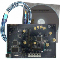
AD9910/PCBZ Analog Devices Inc, AD9910/PCBZ Datasheet - Page 42

AD9910/PCBZ
Manufacturer Part Number
AD9910/PCBZ
Description
Direct Digital Synthesis Evaluation Board
Manufacturer
Analog Devices Inc
Series
AgileRF™r
Specifications of AD9910/PCBZ
Silicon Manufacturer
Analog Devices
Application Sub Type
Direct Digital Synthesizer
Kit Application Type
Clock & Timing
Silicon Core Number
AD9910
Kit Contents
Board
Design Resources
Synchronizing Multiple AD9910 1 GSPS Direct Digital Synthesizers (CN0121)
Main Purpose
Timing, Direct Digital Synthesis (DDS)
Embedded
No
Utilized Ic / Part
AD9910
Primary Attributes
14-Bit DAC, 32-Bit Tuning Word Width
Secondary Attributes
1GHz, Graphical User Interface
Lead Free Status / RoHS Status
Lead free / RoHS Compliant
Lead Free Status / RoHS Status
Lead free / RoHS Compliant, Lead free / RoHS Compliant
Other names
Q3335404
AD9910
ADDITIONAL FEATURES
PROFILES
The AD9910 supports the use of profiles, which consist of a group
of eight registers containing pertinent operating parameters for
a particular operating mode. Profiles enable rapid switching
between parameter sets. Profile parameters are programmed via
the serial I/O port. Once programmed, a specific profile is
activated by means of three external pins (PROFILE[2:0]). A
particular profile is activated by providing the appropriate logic
levels to the profile control pins per Table 15.
Table 15. Profile Control Pins
PROFILE[2:0]
000
001
010
011
100
101
110
111
There are two different parameter sets that the eight profile
registers can control depending on the operating mode of the
device. When RAM enable = 0, the profile parameters follow
the single tone profile format detailed in the Register Map and
Bit Descriptions section. When RAM enable = 1, they follow
the RAM profile format.
As an example of the use of profiles, consider an application for
implementing basic two-tone frequency shift keying (FSK). FSK
uses the binary data in a serial bit stream to select between two
different frequencies: a mark frequency (Logic 1) and a space
frequency (Logic 0). To accommodate FSK, the device operates
in single tone mode. The Single Tone Profile 0 register is pro-
grammed with the appropriate frequency tuning word for a
space. The Single Tone Profile 1 register is programmed with
the appropriate frequency tuning word for a mark. Then, with
the PROFILE1 and PROFILE2 pins tied to Logic 0, the PROFILE0
I/O BUFFERS
THE DEVICE REGISTERS AN I/O UPDATE AT POINT A. THE DATA IS TRANSFERRED FROM THE ASYNCHRONOUSLY LOADED I/O BUFFERS AT POINT B.
I/O_UPDATE
REGISTERS
SYNC_CLK
DATA IN
SYSCLK
DATA IN
N
N – 1
Active Profile
0
1
2
3
4
5
6
7
Figure 49. I/O_UPDATE Transferring Data from I/O Buffer to Active Registers
A
B
N + 1
Rev. C | Page 42 of 64
pin is connected to the serial bit stream. In this way, the logic
state of the PROFILE0 pin causes the appropriate mark and
space frequencies to be generated in accordance with the binary
digits of the bit stream.
The profile pins must meet setup and hold times to the rising
edge of SYNC_CLK.
I/O_UPDATE, SYNC_CLK, AND SYSTEM CLOCK
RELATIONSHIPS
The I/O_UPDATE pin is used to transfer data from the serial
I/O buffer to the active registers in the device. Data in the buffer
is inactive.
SYNC_CLK is a rising edge active signal. It is derived from the
system clock and a divide-by-4 frequency divider. SYNC_CLK,
which is externally provided, can be used to synchronize external
hardware to the AD9910 internal clocks.
I/O_UPDATE initiates the start of a buffer transfer. It can be
sent synchronously or asynchronously relative to the SYNC_CLK.
If the setup time between these signals is met, then constant
latency (pipeline) to the DAC output exists. For example, if
repetitive changes to phase offset via the SPI port is desired,
the latency of those changes to the DAC output is constant;
otherwise, a time uncertainty of one SYNC_CLK period is
present.
By default, the I/O_UPDATE pin is an input that serves as a
strobe signal to allow synchronous update of the device operat-
ing parameters. A rising edge on I/O_UPDATE initiates transfer
of the register contents to the internal workings of the device.
Alternatively, the transfer of programmed data from the program-
ming registers to the internal hardware can be accomplished by
changing the state of the PROFILE[2:0] pins.
The timing diagram shown in Figure 49 depicts when the data
in the buffer is transferred to the active registers.
N
N + 2
N
+ 1


