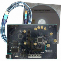
AD9910/PCBZ Analog Devices Inc, AD9910/PCBZ Datasheet - Page 47

AD9910/PCBZ
Manufacturer Part Number
AD9910/PCBZ
Description
Direct Digital Synthesis Evaluation Board
Manufacturer
Analog Devices Inc
Series
AgileRF™r
Specifications of AD9910/PCBZ
Silicon Manufacturer
Analog Devices
Application Sub Type
Direct Digital Synthesizer
Kit Application Type
Clock & Timing
Silicon Core Number
AD9910
Kit Contents
Board
Design Resources
Synchronizing Multiple AD9910 1 GSPS Direct Digital Synthesizers (CN0121)
Main Purpose
Timing, Direct Digital Synthesis (DDS)
Embedded
No
Utilized Ic / Part
AD9910
Primary Attributes
14-Bit DAC, 32-Bit Tuning Word Width
Secondary Attributes
1GHz, Graphical User Interface
Lead Free Status / RoHS Status
Lead free / RoHS Compliant
Lead Free Status / RoHS Status
Lead free / RoHS Compliant, Lead free / RoHS Compliant
Other names
Q3335404
POWER SUPPLY PARTITIONING
The AD9910 features multiple power supplies, and their power
consumption varies with its configuration. This section covers
which power supplies can be grouped together and how the
power consumption of each block varies with frequency.
The values quoted in this section are for comparison only. Refer
to Table 1 for exact values. With each group, use 0.1 μF or 0.01 μF
bypass capacitors in parallel with a 10 μF capacitor.
The recommendations here are for typical applications, for
which there are four groups of power supplies: 3.3 V digital,
3.3 V analog, 1.8 V digital, and 1.8 V analog.
Applications demanding the highest performance may require
additional power supply isolation.
3.3 V SUPPLIES
DVDD_I/O (3.3 V) (Pin 11, Pin 15, Pin 21, Pin 28, Pin 45,
Pin 56, and Pin 66)
These 3.3 V supplies can be grouped together. The power
consumption on these pins varies dynamically with serial port
activity.
AVDD (3.3 V) (Pin 74 to Pin 77 and Pin 83)
These are 3.3 V DAC power supplies that typically consume
about 28 mA. At a minimum, a ferrite bead should be used to
isolate these from other 3.3 V supplies, with a separate regulator
being ideal. The current consumption of these supplies consist
mainly of biasing current and do not vary with frequency.
Rev. C | Page 47 of 64
1.8 V SUPPLIES
DVDD (1.8 V) (Pin 17, Pin 23, Pin 30, Pin 47, Pin 57, and
Pin 64)
These pins can be grouped together. Their current consumption
increases linearly with the system clock frequency. See Figure 17
and Figure 18 for typical current consumption curves. There is
also a slight (~5%) increase as f
400 MHz.
AVDD (1.8 V) (Pin 3)
This 1.8 V supply powers the REFCLK multiplier (PLL) and
consumes about 7 mA. For applications demanding the highest
performance with the PLL enabled, this supply should be
isolated from other 1.8 V AVDD supplies with a separate
regulator. For less demanding applications, this supply can be
run off the same regulator as Pin 89 and Pin 92 with a ferrite
bead to isolate Pin 3 from Pin 89 and Pin 92.
The loop filter for the PLL should directly connect to Pin 3. If
the PLL is bypassed, Pin 3 should still be powered, but isolation
is not critical.
AVDD (1.8 V) (Pin 6)
This pin can be grouped together with the DVDD 1.8 V supply
pins. For the highest performance, a ferrite bead should be used
for isolation, with a separate regulator being ideal.
AVDD (1.8 V) (Pin 89 and Pin 92)
This 1.8 V supply for the REFCLK input consumes about
15 mA. These pins can run off the supply of Pin 3 with a ferrite
bead to isolate Pin 3 from Pin 89 and Pin 92. At a minimum, a
ferrite bead should be used to isolate these from other 1.8 V
supplies. However, for applications demanding the highest
performance, a separate regulator is recommended.
OUT
increases from 50 MHz to
AD9910


