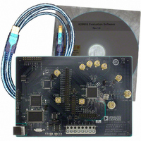
AD9910/PCBZ Analog Devices Inc, AD9910/PCBZ Datasheet - Page 34

AD9910/PCBZ
Manufacturer Part Number
AD9910/PCBZ
Description
Direct Digital Synthesis Evaluation Board
Manufacturer
Analog Devices Inc
Series
AgileRF™r
Specifications of AD9910/PCBZ
Silicon Manufacturer
Analog Devices
Application Sub Type
Direct Digital Synthesizer
Kit Application Type
Clock & Timing
Silicon Core Number
AD9910
Kit Contents
Board
Design Resources
Synchronizing Multiple AD9910 1 GSPS Direct Digital Synthesizers (CN0121)
Main Purpose
Timing, Direct Digital Synthesis (DDS)
Embedded
No
Utilized Ic / Part
AD9910
Primary Attributes
14-Bit DAC, 32-Bit Tuning Word Width
Secondary Attributes
1GHz, Graphical User Interface
Lead Free Status / RoHS Status
Lead free / RoHS Compliant
Lead Free Status / RoHS Status
Lead free / RoHS Compliant, Lead free / RoHS Compliant
Other names
Q3335404
AD9910
During playback, the state machine uses an up/down counter to
step through the specified address locations. The clock rate of
this counter defines the playback rate, that is, the sample rate of
the generated waveform. The clocking of the counter is controlled
by a 16-bit programmable timer that is internal to the state
machine. This timer is clocked by the DDS clock, and its time
interval is set by the 16-bit address step rate value stored in the
selected RAM profile register.
The address step rate value determines the playback rate. For
example, if M is the 16-bit value of the address step rate for a
specific RAM profile, then the playback rate for that profile is
given by
The sample interval (Δt) associated with the playback rate is
therefore given by
RAM data entry/retrieval via the I/O port takes precedence
over playback operation. An I/O operation targeting the RAM
during playback interrupts any waveform in progress.
The 32-bit words output by the RAM during playback route to
the DDS signal control parameters according to two RAM
playback destination bits in Control Function Register 1. The
32-bit words are partitioned based on Table 12.
Table 12. RAM Playback Destination
RAM Playback
Destination Bits
CFR1[30:29]
00
01
10
11
When the destination is phase, amplitude, or polar, the unused
LSBs are ignored.
10
Δ
Playback
t
10
WAVEFORM START ADDRESS
DDS CLOCK
MACHINE
=
WAVEFORM END ADDRESS
STATE
16
Playback
ADDRESS RAMP RATE
3
Rate
2
1
Figure 42. RAM Playback Operation
=
Rate
COUNTER
UP/DOWN
RAM MODE
f
NO DWELL
U/D
DDSCLOCK
DDS Signal
Control
Parameter
Frequency
Phase
Amplitude
Polar (phase
and amplitude)
Q
=
M
10
f
SYSCLK
4
M
=
REGISTERS
PROFILE
f
RAM
SYSCLK
RAM
4
M
Bits Assigned to
DDS Parameters
31:0
31:16
31:18
31:16 (phase)
15:2 (amplitude)
32
3
TO DDS
SIGNAL
CONTROL
PARAMETER
PROFILE
Rev. C | Page 34 of 64
The RAM playback destination bits affect specific DDS signal
control parameters. The parameters that are not affected by the
RAM playback destination bits are controlled by the FTW, POW,
and/or ASF registers.
RAM_SWP_OVR (RAM Sweep Over) Pin
The RAM_SWP_OVR pin provides an active high external
signal that indicates the end of a playback sequence. The
operation of this pin varies with the RAM operating mode
as detailed in the following sections. When RAM enable = 0,
this pin is forced to a Logic 0.
Overview of RAM Playback Modes
The RAM can operate in any one of five different playback modes.
•
•
•
•
•
The mode is selected via the 3-bit RAM mode control word
located in each of the RAM profile registers. Thus, the RAM
operating mode is profile dependent. The RAM profile mode
control bits are detailed in Table 13.
Table 13. RAM Operating Modes
RAM Profile
Mode Control Bits
000, 101, 110, 111
001
010
011
100
RAM Direct Switch Mode
In direct switch mode, the RAM is not used as a waveform genera-
tor. Instead, when a RAM profile is selected via the PROFILE[2:0]
pins, only a single 32-bit word is routed to the DDS to be applied
to the signal control parameter(s). This 32-bit word is the data
stored in the RAM at the location given by the 10-bit waveform
start address of the selected profile.
In direct switch mode, the RAM_SWP_OVR pin is always
Logic 0, and the no-dwell high bit is ignored.
Direct switch mode enables up to eight-level FSK, PSK, or ASK
modulation; the type of modulation is determined by the RAM
playback destination bits (frequency for FSK and so on). Each
RAM profile is associated with a specific value of frequency,
phase, or amplitude. Each unique waveform start address value
in each RAM profile allows access of the 32-bit word stored in
that particular RAM location. In this way, the profile pins
implement the shift-keying function, modulating the DDS
output as desired.
Direct switch
Ramp-up
Bidirectional ramp
Continuous bidirectional ramp
Continuous recirculate
RAM Operating Mode
Direct switch
Ramp-up
Bidirectional ramp
Continuous bidirectional ramp
Continuous recirculate


