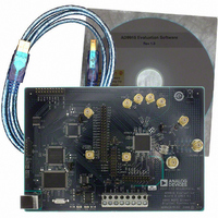
AD9910/PCBZ Analog Devices Inc, AD9910/PCBZ Datasheet - Page 43

AD9910/PCBZ
Manufacturer Part Number
AD9910/PCBZ
Description
Direct Digital Synthesis Evaluation Board
Manufacturer
Analog Devices Inc
Series
AgileRF™r
Specifications of AD9910/PCBZ
Silicon Manufacturer
Analog Devices
Application Sub Type
Direct Digital Synthesizer
Kit Application Type
Clock & Timing
Silicon Core Number
AD9910
Kit Contents
Board
Design Resources
Synchronizing Multiple AD9910 1 GSPS Direct Digital Synthesizers (CN0121)
Main Purpose
Timing, Direct Digital Synthesis (DDS)
Embedded
No
Utilized Ic / Part
AD9910
Primary Attributes
14-Bit DAC, 32-Bit Tuning Word Width
Secondary Attributes
1GHz, Graphical User Interface
Lead Free Status / RoHS Status
Lead free / RoHS Compliant
Lead Free Status / RoHS Status
Lead free / RoHS Compliant, Lead free / RoHS Compliant
Other names
Q3335404
AUTOMATIC I/O UPDATE
The AD9910 offers an option whereby the I/O update function
is asserted automatically rather than relying on an external signal
supplied by the user. This feature is enabled by setting the internal
I/O update active bit in Control Function Register 2 (CFR2).
When this feature is active, the I/O_UPDATE pin becomes an
output pin. It generates an active high pulse each time an inter-
nal I/O update occurs. The pulse width is determine by the I/O
update rate control bits (CFR2[15:14]). Table 16 approximates the
pulse width setting.
Table 16. Pulse Width Setting
I/O Update Rate Control Bits
(CFR2[15:14])
00
01
10
11
This I/O update strobe can be used to notify an external
controller that the device has generated an I/O update
internally.
The repetition rate of the internal I/O update is programmed
via the serial I/O port. There are two parameters that control
the repetition rate. The first consists of the two I/O update rate
control bits in CFR2. The second is the 32-bit word in the I/O
update rate register that sets the range of an internal counter.
The I/O update rate control bits establish a divide-by-1, -2, -4,
or -8 of a clock signal that runs at ¼ f
divider clocks the aforementioned 32-bit internal counter. The
repetition rate of the I/O update is given by
where:
A is the value of the 2-bit word comprising the I/O update rate
control bits.
B is the value of the 32-bit word stored in the I/O update rate
register.
The default value of A is 0, and the value of B is 0xFFFF. If B is
programmed to 0x0003 or less, the I/O_UPDATE pin no longer
pulses but assumes a static Logic 1 state.
f
I
/
O
_
UPDATE
=
f
2
SYSCLK
A
+
2
B
SYSCLK
I/O Update Pulse Width
12 SYSCLKs
24 SYSCLKs
48 SYSCLKs
96 SYSCLKs
. The output of the
Rev. C | Page 43 of 64
POWER-DOWN CONTROL
The AD9910 offers the ability to independently power down
four specific sections of the device. Power-down functionality
applies to the following:
•
•
•
•
A power-down of the digital core disables the ability to update
the serial I/O port. However, the digital power-down bit can
still be cleared via the serial port to prevent the possibility of a
nonrecoverable state.
Software power-down is controlled via four independent power-
down bits in Control Function Register 1 (CFR1). Software
control requires that the EXT_PWR_DWN pin be forced to a
Logic 0 state. In this case, setting the desired power-down bits
(via the serial I/O port) powers down the associated functional
block, whereas clearing the bits restores the function.
Alternatively, all four functions can be simultaneously powered
down via external hardware control through the EXT_PWR_DWN
pin. When this pin is forced to Logic 1, all four circuit blocks are
powered down regardless of the state of the power-down bits;
that is, the independent power-down bits in CFR1 are ignored
and overridden when EXT_PWR_DWN is Logic 1.
Based on the state of the external power-down control bit, the
EXT_PWR_DWN pin produces either a full power-down or a
fast recovery power-down. The fast recovery power-down mode
maintains power to the DAC bias circuitry and the PLL, VCO,
and input clock circuitry. Although the fast recovery power-
down does not conserve as much power as the full power-down,
it allows the device to awaken very quickly from the power-
down state.
Digital core
DAC
Auxiliary DAC
Input REFCLK clock circuitry
AD9910


