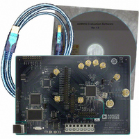
AD9910/PCBZ Analog Devices Inc, AD9910/PCBZ Datasheet - Page 26

AD9910/PCBZ
Manufacturer Part Number
AD9910/PCBZ
Description
Direct Digital Synthesis Evaluation Board
Manufacturer
Analog Devices Inc
Series
AgileRF™r
Specifications of AD9910/PCBZ
Silicon Manufacturer
Analog Devices
Application Sub Type
Direct Digital Synthesizer
Kit Application Type
Clock & Timing
Silicon Core Number
AD9910
Kit Contents
Board
Design Resources
Synchronizing Multiple AD9910 1 GSPS Direct Digital Synthesizers (CN0121)
Main Purpose
Timing, Direct Digital Synthesis (DDS)
Embedded
No
Utilized Ic / Part
AD9910
Primary Attributes
14-Bit DAC, 32-Bit Tuning Word Width
Secondary Attributes
1GHz, Graphical User Interface
Lead Free Status / RoHS Status
Lead free / RoHS Compliant
Lead Free Status / RoHS Status
Lead free / RoHS Compliant, Lead free / RoHS Compliant
Other names
Q3335404
AD9910
loop filter components (connected via the PLL_LOOP_FILTER
pin). These features add an extra layer of flexibility to the PLL,
allowing optimization of phase noise performance and
flexibility in frequency plan development. The PLL is also
equipped with a PLL_LOCK pin.
The PLL output frequency range (f
range of 420 MHz ≤ f
addition, the user must program the VCO to one of six operating
ranges such that f
and Figure 34 summarize these VCO ranges.
Figure 33 shows the boundaries of the VCO frequency ranges
over the full range of temperature and supply voltage variation
for all devices from the available population. The implication is
that multiple devices chosen at random from the population and
operated under widely varying conditions may require different
values to be programmed into CFR3[26:24] to operate at the
same frequency. For example, Part A chosen randomly from the
population, operating at an ambient temperature of −10°C with
a system clock frequency of 900 MHz may require CFR3[26:24] to
be set to 100b, whereas Part B chosen randomly from the
population, operating at an ambient temperature of 90°C with a
system clock frequency of 900 MHz may require CFR3[26:24]
to be set to 101b. If a frequency plan is chosen such that the
system clock frequency operates within one set of boundaries
(as shown in Figure 33), the required value in CFR3[26:24] is
consistent from part to part.
Figure 34 shows the boundaries of the VCO frequency ranges
over the full range of temperature and supply voltage variation
for an individual device selected from the population. Figure 34
shows that the VCO frequency ranges for a single device always
overlap when operated over the full range of conditions.
If a user wants to retain a single default value for CFR3[26:24],
a frequency that falls into one of the ranges found in Figure 33
should be selected. Additionally, for any given individual device,
the VCO frequency ranges overlap, meaning that any given
device exhibits no gaps in its frequency coverage across VCO
ranges over the full range of conditions.
VCO5
VCO4
VCO3
VCO2
VCO1
VCO0
Figure 33. VCO Ranges Including Atypical Wafer Process Skew
395
f
f
LOW
HIGH
495
SYSCLK
= 400
= 460
f
f
LOW
HIGH
SYSCLK
falls within the specified range. Figure 33
595
= 455
= 530
≤ 1 GHz by the internal VCO. In
f
f
f
f
LOW
HIGH
HIGH
LOW
695
= 530
= 615
(MHz)
= 760
= 875
SYSCLK
795
f
HIGH
f
f
f
) is constrained to the
LOW
LOW
HIGH
= 1030
= 920
= 650
= 790
895
995
Rev. C | Page 26 of 64
Table 8. VCO Range Bit Settings
VCO SEL Bits (CFR3[26:24])
000
001
010
011
100
101
110
111
PLL Charge Pump
The charge pump current (I
user with additional flexibility to optimize the PLL performance.
Table 9 lists the bit settings vs. the nominal charge pump current.
Table 9. PLL Charge Pump Current
I
000
001
010
011
100
101
110
111
CP
Bits (CFR3[21:19])
VCO5
VCO4
VCO3
VCO2
VCO1
VCO0
335
435
Figure 34. Typical VCO Ranges
535
f
f
f
LOW
HIGH
f
HIGH
LOW
= 370
= 510
= 700
= 950
f
f
635
LOW
HIGH
Charge Pump Current, I
212
237
262
287
312
337
363
387
f
CP
HIGH
f
= 420
LOW
= 590
) is programmable to provide the
f
f
735
LOW
HIGH
(MHz)
= 1150
= 820
= 500
= 700
835
f
f
LOW
HIGH
935
VCO Range
VCO0
VCO1
VCO2
VCO3
VCO4
VCO5
PLL bypassed
PLL bypassed
= 600
= 880
1035
CP
1135
(μA)


