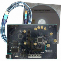
AD9910/PCBZ Analog Devices Inc, AD9910/PCBZ Datasheet - Page 55

AD9910/PCBZ
Manufacturer Part Number
AD9910/PCBZ
Description
Direct Digital Synthesis Evaluation Board
Manufacturer
Analog Devices Inc
Series
AgileRF™r
Specifications of AD9910/PCBZ
Silicon Manufacturer
Analog Devices
Application Sub Type
Direct Digital Synthesizer
Kit Application Type
Clock & Timing
Silicon Core Number
AD9910
Kit Contents
Board
Design Resources
Synchronizing Multiple AD9910 1 GSPS Direct Digital Synthesizers (CN0121)
Main Purpose
Timing, Direct Digital Synthesis (DDS)
Embedded
No
Utilized Ic / Part
AD9910
Primary Attributes
14-Bit DAC, 32-Bit Tuning Word Width
Secondary Attributes
1GHz, Graphical User Interface
Lead Free Status / RoHS Status
Lead free / RoHS Compliant
Lead Free Status / RoHS Status
Lead free / RoHS Compliant, Lead free / RoHS Compliant
Other names
Q3335404
REGISTER BIT DESCRIPTIONS
The serial I/O port registers span an address range of 0 to 23
(0x00 to 0x16 in hexadecimal notation). This represents a total
of 24 registers. However, two of these registers are unused,
yielding a total of 22 available registers. The unused registers are
Register 5 and Register 6 (0x05 and 0x06, respectively).
The number of bytes assigned to the registers varies. That is, the
registers are not of uniform depth; each contains the number of
bytes necessary for its particular function. Additionally, the
registers are assigned names according to their functionality. In
some cases, a register is given a mnemonic descriptor. For
example, the register at Serial Address 0x00 is named Control
Function Register 1 and is assigned the mnemonic CFR1.
The following section provides a detailed description of each bit
in the AD9910 register map. For cases in which a group of bits
serves a specific function, the entire group is considered a
binary word and described in aggregate.
Control Function Register 1 (CFR1)—Address 0x00
Four bytes are assigned to this register.
Table 18. Bit Description for CFR1
Bit(s)
31
30:29
28:24
23
22
21
20:17
16
15
14
13
Mnemonic
RAM enable
RAM playback destination
Open
Manual OSK external
control
Inverse sinc filter enable
Open
Internal profile control
Select DDS sine output
Load LRR @ I/O update
Autoclear digital ramp
accumulator
Autoclear phase
accumulator
Description
0 = disables RAM functionality (default).
1 = enables RAM functionality (required for both load/retrieve and playback operation).
See Table 12 for details; default is 00b.
Ineffective unless CFR1[9:8] = 10b.
0 = inverse sinc filter bypassed (default).
1 = inverse sinc filter active.
Ineffective unless CFR1[31] = 1. These bits are effective without the need for an I/O update.
See Table 14 for details. Default is 0000b.
0 = cosine output of the DDS is selected (default).
1 = sine output of the DDS is selected.
Ineffective unless CFR2[19] = 1.
0 = normal operation of the DRG accumulator (default).
1 = the ramp accumulator is reset for one cycle of the DDS clock after which the accumula-
tor automatically resumes normal operation. As long as this bit remains set, the ramp
accumulator is momentarily reset each time an I/O_UPDATE is asserted or a PROFILE[2:0]
change occurs. This bit is synchronized with either an I/O _UPDATE or a PROFILE[2:0]
change and the next rising edge of SYNC_CLK.
0 = normal operation of the DDS phase accumulator (default).
1 = synchronously resets the DDS phase accumulator anytime I/O_UPDATE is asserted or a
profile change occurs.
0 = OSK pin inoperative (default).
1 = OSK pin enabled for manual OSK control (see Output Shift Keying (OSK) section for
details).
0 = normal operation of the digital ramp timer (default).
1 = digital ramp timer loaded any time I/O_UPDATE is asserted or a PROFILE[2:0] change
occurs.
Rev. C | Page 55 of 64
This section is organized in sequential order of the serial addresses
of the registers. Each subheading includes the register name and
optional register mnemonic (in parentheses). Also given is the
serial address in hexadecimal format and the number of bytes
assigned to the register.
Following each subheading is a table containing the individual
bit descriptions for that particular register. The location of the
bit(s) in the register is indicated by a single number or a pair of
numbers separated by a colon; that is, a pair of numbers (A:B)
indicates a range of bits from the most significant (A) to the
least significant (B). For example, 5:2 implies Bit Position 5
down to Bit Position 2, inclusive, with Bit 0 identifying the LSB
of the register.
Unless otherwise stated, programmed bits are not transferred to
their internal destinations until the assertion of the I/O_UPDATE
pin or a profile change.
AD9910


