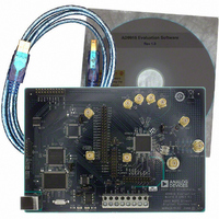
AD9910/PCBZ Analog Devices Inc, AD9910/PCBZ Datasheet - Page 57

AD9910/PCBZ
Manufacturer Part Number
AD9910/PCBZ
Description
Direct Digital Synthesis Evaluation Board
Manufacturer
Analog Devices Inc
Series
AgileRF™r
Specifications of AD9910/PCBZ
Silicon Manufacturer
Analog Devices
Application Sub Type
Direct Digital Synthesizer
Kit Application Type
Clock & Timing
Silicon Core Number
AD9910
Kit Contents
Board
Design Resources
Synchronizing Multiple AD9910 1 GSPS Direct Digital Synthesizers (CN0121)
Main Purpose
Timing, Direct Digital Synthesis (DDS)
Embedded
No
Utilized Ic / Part
AD9910
Primary Attributes
14-Bit DAC, 32-Bit Tuning Word Width
Secondary Attributes
1GHz, Graphical User Interface
Lead Free Status / RoHS Status
Lead free / RoHS Compliant
Lead Free Status / RoHS Status
Lead free / RoHS Compliant, Lead free / RoHS Compliant
Other names
Q3335404
Control Function Register 2 (CFR2)—Address 0x01
Four bytes are assigned to this register.
Table 19. Bit Descriptions for CFR2
Bit(s)
31:25
24
23
22
21:20
19
18
17
16
15:14
13:12
11
10
9
8
7
Mnemonic
Open
Enable amplitude scale
from single tone profiles
Internal I/O update active
SYNC_CLK enable
Digital ramp destination
Digital ramp enable
Digital ramp no-dwell high
Digital ramp no-dwell low
Read effective FTW
I/O update rate control
Open
PDCLK enable
PDCLK invert
TxEnable invert
Open
Matched latency enable
Description
Ineffective if CFR2[19 ] = 1 or CFR1[31] = 1 or CFR1[9] = 1.
This bit is effective without the need for an I/O update.
0 = the SYNC_CLK pin is disabled; static Logic 0 output.
1 = the SYNC_CLK pin generates a clock signal at ¼ f
serial I/O port (default).
See Table 11 for details. Default is 00b. See the Digital Ramp Generator (DRG) section for
details.
0 = disables digital ramp generator functionality (default).
1 = enables digital ramp generator functionality.
See the Digital Ramp Generator (DRG) section for details.
See the Digital Ramp Generator (DRG) section for details.
0 = a serial I/O port read operation of the FTW register reports the contents of the FTW
register (default).
1 = a serial I/O port read operation of the FTW register reports the actual 32-bit word
appearing at the input to the DDS phase accumulator.
Ineffective unless CFR2[23] = 1. Sets the prescale ratio of the divider that clocks the auto I/O
update timer as follows:
0 = the PDCLK pin is disabled and forced to a static Logic 0 state; the internal clock signal
continues to operate and provide timing to the data assembler.
1 = the internal PDCLK signal appears at the PDCLK pin (default).
0 = normal PDCLK polarity; Q-data associated with Logic 1, I-data with Logic 0 (default).
1 = inverted PDCLK polarity.
0 = no inversion.
1 = inversion.
0 = simultaneous application of amplitude, phase, and frequency changes to the DDS
arrive at the output in the order listed (default).
1 = simultaneous application of amplitude, phase, and frequency changes to the DDS
arrive at the output simultaneously.
0 = the amplitude scaler is bypassed and shut down for power conservation (default).
1 = the amplitude is scaled by the ASF from the active profile.
0 = serial I/O programming is synchronized with the external assertion of the
I/O_UPDATE pin, which is configured as an input pin (default).
1 = serial I/O programming is synchronized with an internally generated I/O update
signal (the internally generated signal appears at the I/O_UPDATE pin, which is
configured as an output pin).
0 = disables no-dwell high functionality (default).
1 = enables no-dwell high functionality.
0 = disables no-dwell low functionality (default).
1 = enables no-dwell low functionality.
00 = divide-by-1 (default).
01 = divide-by-2.
10 = divide-by-4.
11 = divide-by-8.
Rev. C | Page 57 of 64
SYSCLK
; used for synchronization of the
AD9910


