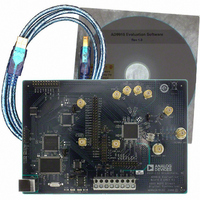
AD9910/PCBZ Analog Devices Inc, AD9910/PCBZ Datasheet - Page 28

AD9910/PCBZ
Manufacturer Part Number
AD9910/PCBZ
Description
Direct Digital Synthesis Evaluation Board
Manufacturer
Analog Devices Inc
Series
AgileRF™r
Specifications of AD9910/PCBZ
Silicon Manufacturer
Analog Devices
Application Sub Type
Direct Digital Synthesizer
Kit Application Type
Clock & Timing
Silicon Core Number
AD9910
Kit Contents
Board
Design Resources
Synchronizing Multiple AD9910 1 GSPS Direct Digital Synthesizers (CN0121)
Main Purpose
Timing, Direct Digital Synthesis (DDS)
Embedded
No
Utilized Ic / Part
AD9910
Primary Attributes
14-Bit DAC, 32-Bit Tuning Word Width
Secondary Attributes
1GHz, Graphical User Interface
Lead Free Status / RoHS Status
Lead free / RoHS Compliant
Lead Free Status / RoHS Status
Lead free / RoHS Compliant, Lead free / RoHS Compliant
Other names
Q3335404
AD9910
Automatic OSK
In automatic mode, the OSK function automatically generates a
linear amplitude vs. time profile (or amplitude ramp). The ampli-
tude ramp is controlled via three parameters: the maximum
amplitude scale factor, the amplitude step size, and the time
interval between steps. The amplitude ramp parameters reside
in the 32-bit ASF register and are programmed via the serial
I/O port. The time interval between amplitude steps is set via
the 16-bit amplitude ramp rate portion of the ASF register
(Bits[31:16]). The maximum amplitude scale factor is set via the
14-bit amplitude scale factor in the ASF register (Bits[15:2]). The
amplitude step size is set via the 2-bit amplitude step size
portion of the ASF register (Bits[1:0]). Additionally, the
direction of the ramp (positive or negative slope) is controlled
by the external OSK pin.
The step interval is controlled by a 16-bit programmable timer
that is clocked at a rate of ¼ f
the time interval between amplitude steps. The step time interval
(Δt) is given by
where M is the 16-bit number stored in the amplitude ramp rate
(ARR) portion of the ASF register. For example, if f
750 MHz and M = 23218 (0x5AB2), then Δt ≈ 123.8293 μs.
The output of the OSK function is a 14-bit unsigned data bus
that controls the amplitude parameter of the DDS (as long as
the OSK enable bit is set). When the OSK pin is set, the OSK
output value starts at 0 (zero) and increments by the pro-
grammed amplitude step size until it reaches the programmed
maximum amplitude value. When the OSK pin is cleared, the
OSK output starts at its present value and decrements by the
programmed amplitude step size until it reaches 0 (zero).
The OSK output does not necessarily attain the maximum
amplitude value if the OSK pin is switched to Logic 0 before the
maximum value is reached. Nor does the OSK output necessarily
reach a value of 0 if the OSK pin is switched to Logic 1 before
the 0 value is reached.
The OSK output is initialized to 0 (zero) at power-up and reset
whenever the OSK enable bit or the select auto OSK bit is cleared.
The amplitude step size of the OSK output is set by the amplitude
step size bits in the ASF register according to Table 10. The step
size refers to the LSB weight of the 14-bit OSK output. Regardless
of the programmed step size, the OSK output does not exceed
the maximum amplitude value programmed into the ASF
register.
Δ =
t
f
SYSCLK
4
M
SYSCLK
. The period of the timer sets
SYSCLK
=
Rev. C | Page 28 of 64
Table 10. OSK Amplitude Step Size
Amplitude Step Size Bits (ASF[1:0])
00
01
10
11
As mentioned previously, a 16-bit programmable timer controls
the step interval. Normally, this timer is loaded with the pro-
grammed timing value whenever the timer expires, initiating a
new timing cycle. However, there are three events that can cause
reloading of the timer to have its timing value reloaded prior to
the timer expiring. One such event occurs when the select auto
OSK bit transitions from cleared to set, followed by an I/O update.
A second such event is a change of state in the OSK pin. The
third is dependent on the status of the load ARR @ I/O update
bit. If this bit is cleared, then no action occurs; otherwise, when
the I/O_UPDATE pin is asserted (or a profile change occurs),
the timer is reset to its initial starting point.
DIGITAL RAMP GENERATOR (DRG)
DRG Overview
To sweep phase, frequency, or amplitude from a defined start
point to a defined endpoint, a completely digital, digital ramp
generator is included in the AD9910. The DRG makes use of
nine control register bits, three external pins, two 64-bit
registers, and one 32-bit register (see Figure 37).
DIGITAL RAMP LIMIT REGISTER
DIGITAL RAMP RATE REGISTER
DIGITAL RAMP STEP REGISTER
DIGITAL RAMP DESTINATION
LOAD LRR AT I/O_UPDATE
DIGITAL RAMP NO-DWELL
DIGITAL RAMP ENABLE
RAMP ACCUMULATOR
RAMP ACCUMULATOR
AUTOCLEAR DIGITAL
DROVER PIN ACTIVE
CLEAR DIGITAL
Figure 37. Digital Ramp Block Diagram
64
64
32
2
2
GENERATOR
62
DDS CLOCK
DIGITAL
RAMP
61
Amplitude Step Size
1
2
4
8
63
32
TO DDS
SIGNAL
CONTROL
PARAMETER


