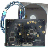
AD9910/PCBZ Analog Devices Inc, AD9910/PCBZ Datasheet - Page 16

AD9910/PCBZ
Manufacturer Part Number
AD9910/PCBZ
Description
Direct Digital Synthesis Evaluation Board
Manufacturer
Analog Devices Inc
Series
AgileRF™r
Specifications of AD9910/PCBZ
Silicon Manufacturer
Analog Devices
Application Sub Type
Direct Digital Synthesizer
Kit Application Type
Clock & Timing
Silicon Core Number
AD9910
Kit Contents
Board
Design Resources
Synchronizing Multiple AD9910 1 GSPS Direct Digital Synthesizers (CN0121)
Main Purpose
Timing, Direct Digital Synthesis (DDS)
Embedded
No
Utilized Ic / Part
AD9910
Primary Attributes
14-Bit DAC, 32-Bit Tuning Word Width
Secondary Attributes
1GHz, Graphical User Interface
Lead Free Status / RoHS Status
Lead free / RoHS Compliant
Lead Free Status / RoHS Status
Lead free / RoHS Compliant, Lead free / RoHS Compliant
Other names
Q3335404
AD9910
APPLICATION CIRCUITS
Figure 20. Synchronizing Multiple Devices to Increase Channel Capacity Using the AD9510 as a Clock Distributor for the Reference and Synchronization Clock
Figure 21. Clock Generation Circuit Using the AD9512/AD9513/AD9514/AD9515 Series of Clock Distribution Chips
n = DEPENDENT ON PRODUCT SELECTION.
REFCLK
REFERENCE
Figure 19. DDS in PLL Feedback Locking to Reference, Offering Fine Frequency and Delay Adjust Tuning
CENTRAL
CONTROL
÷
÷
AD9910
AD9510, AD9511, ADF4106
FPGA
FPGA
FPGA
FPGA
LPF
SOURCE
COMPARATOR
CLOCK
DELAY EQUALIZATION
PHASE
SYNCHRONIZATION
SYNC_CLK
SYNC_CLK
SYNC_CLK
DATA
DATA
DATA
DATA
CH 2
SYNC_CLK
Rev. C | Page 16 of 64
AD9510
AD9910
DELAY EQUALIZATION
CLOCK DISTRIBUTOR
LPF
CHARGE
PUMP
AD9510
WITH
DIVIDER AND DELAY ADJUST
PROGRAMMABLE 1 TO 32
REF_CLK
REF_CLK
C1
S1
C2
S2
C3
S3
C4
S4
AD9515
AD9514
AD9513
AD9512
AD9910
(MASTER)
AD9910
AD9910
AD9910
(SLAVE 1)
(SLAVE 2)
(SLAVE 3)
FILTER
LOOP
SYNC_OUT
n
VCO
A1
A2
A3
A4
CLOCK OUTPUT
A_END
SELECTION(S)
LVPECL
CMOS
LVDS


