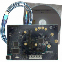
AD9910/PCBZ Analog Devices Inc, AD9910/PCBZ Datasheet - Page 5

AD9910/PCBZ
Manufacturer Part Number
AD9910/PCBZ
Description
Direct Digital Synthesis Evaluation Board
Manufacturer
Analog Devices Inc
Series
AgileRF™r
Specifications of AD9910/PCBZ
Silicon Manufacturer
Analog Devices
Application Sub Type
Direct Digital Synthesizer
Kit Application Type
Clock & Timing
Silicon Core Number
AD9910
Kit Contents
Board
Design Resources
Synchronizing Multiple AD9910 1 GSPS Direct Digital Synthesizers (CN0121)
Main Purpose
Timing, Direct Digital Synthesis (DDS)
Embedded
No
Utilized Ic / Part
AD9910
Primary Attributes
14-Bit DAC, 32-Bit Tuning Word Width
Secondary Attributes
1GHz, Graphical User Interface
Lead Free Status / RoHS Status
Lead free / RoHS Compliant
Lead Free Status / RoHS Status
Lead free / RoHS Compliant, Lead free / RoHS Compliant
Other names
Q3335404
GENERAL DESCRIPTION
The AD9910 is a direct digital synthesizer (DDS) featuring
an integrated 14-bit DAC and supporting sample rates up to
1 GSPS. The AD9910 employs an advanced, proprietary DDS
technology that provides a significant reduction in power con-
sumption without sacrificing performance. The DDS/DAC
combination forms a digitally programmable, high frequency,
analog output synthesizer capable of generating a frequency
agile sinusoidal waveform at frequencies up to 400 MHz.
The user has access to the three signal control parameters that
control the DDS: frequency, phase, and amplitude. The DDS
provides fast frequency hopping and frequency tuning resolu-
tion with its 32-bit accumulator. With a 1 GSPS sample rate, the
tuning resolution is ~0.23 Hz. The DDS also enables fast phase
and amplitude switching capability.
PROFILE[2:0]
I/O_UPDATE
I/O_RESET
PARALLEL
TxENABLE
DRHOLD
DROVER
PDCLK
DRCTL
INPUT
SCLK
SDIO
OSK
CS
16
2
2
2
3
PARALLEL DATA
TIMING AND
CONTROL
PROGRAMMING
REGISTERS
8
RAM_SWP_OVR
GENERATOR
DAC FSC
OUTPUT
KEYING
DIGITAL
SHIFT
RAMP
RAM
PARTITION
CONTROL
ROUTE
DATA
AND
Figure 2. Detailed Block Diagram
AMPLITUDE (A)
PHASE (θ)
FREQUENCY (ω)
Rev. C | Page 5 of 64
INTERNAL CLOCK TIMING
AND CONTROL
AD9910
CONTROL
POWER-
DOWN
CLOCK
ω
A
θ
DDS
The AD9910 is controlled by programming its internal control
registers via a serial I/O port. The AD9910 includes an integrated
static RAM to support various combinations of frequency, phase,
and/or amplitude modulation. The AD9910 also supports a user
defined, digitally controlled, digital ramp mode of operation. In
this mode, the frequency, phase, or amplitude can be varied
linearly over time. For more advanced modulation functions, a
high speed parallel data input port is included to enable direct
frequency, phase, amplitude, or polar modulation.
The AD9910 is specified to operate over the extended industrial
temperature range (see the Absolute Maximum Ratings section
for details).
Acos (ωt + θ)
Asin (ωt + θ)
SYNCHRONIZATION
MULTICHIP
SYSCLK
DAC FSC
2
2
INVERSE
FILTER
SINC
8
PLL
÷2
8-BIT
AUX
DAC
14-BIT
DAC
DAC_RSET
IOUT
IOUT
REFCLK_OUT
REF_CLK
REF_CLK
XTAL_SEL
AD9910


