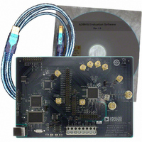
AD9910/PCBZ Analog Devices Inc, AD9910/PCBZ Datasheet - Page 20

AD9910/PCBZ
Manufacturer Part Number
AD9910/PCBZ
Description
Direct Digital Synthesis Evaluation Board
Manufacturer
Analog Devices Inc
Series
AgileRF™r
Specifications of AD9910/PCBZ
Silicon Manufacturer
Analog Devices
Application Sub Type
Direct Digital Synthesizer
Kit Application Type
Clock & Timing
Silicon Core Number
AD9910
Kit Contents
Board
Design Resources
Synchronizing Multiple AD9910 1 GSPS Direct Digital Synthesizers (CN0121)
Main Purpose
Timing, Direct Digital Synthesis (DDS)
Embedded
No
Utilized Ic / Part
AD9910
Primary Attributes
14-Bit DAC, 32-Bit Tuning Word Width
Secondary Attributes
1GHz, Graphical User Interface
Lead Free Status / RoHS Status
Lead free / RoHS Compliant
Lead Free Status / RoHS Status
Lead free / RoHS Compliant, Lead free / RoHS Compliant
Other names
Q3335404
AD9910
PARALLEL DATA PORT MODULATION MODE
In parallel data port modulation mode (see Figure 25), the
modulated DDS signal control parameter(s) are supplied
directly from the 18-bit parallel data port.
The data port is partitioned into two sections. The 16 MSBs make
up a 16-bit data-word (D[15:0] pins) and the two LSBs make up
a 2-bit destination word (F[1:0] pins). The destination word
defines how the 16-bit data-word is applied to the DDS signal
control parameters. Table 4 defines the relationship between the
destination bits, the partitioning of the 16-bit data-word, and
the destination of the data (in terms of the DDS signal control
parameters). Formatting of the 16-bit data-word is unsigned
binary, regardless of the destination.
When the destination bits indicate that the data-word is destined
as a DDS frequency parameter, the 16-bit data-word serves as
an offset to the 32-bit frequency tuning word in the FTW regis-
ter. This means that the 16-bit data-word must somehow be
properly aligned with the 32-bit word in the FTW register. This
is accomplished by means of the 4-bit FM gain word in the
programming registers. The FM gain word allows the user to
PROFILE[2:0]
I/O_UPDATE
I/O_RESET
PARALLEL
TxENABLE
DRHOLD
DROVER
PDCLK
DRCTL
INPUT
SCLK
SDIO
OSK
CS
16
2
2
2
3
PARALLEL DATA
TIMING AND
CONTROL
PROGRAMMING
REGISTERS
8
RAM_SWP_OVR
GENERATOR
DAC FSC
OUTPUT
KEYING
DIGITAL
SHIFT
RAMP
RAM
PARTITION
CONTROL
ROUTE
Figure 25. Parallel Data Port Modulation Mode
DATA
AND
AMPLITUDE (A)
PHASE (θ)
FREQUENCY (ω)
Rev. C | Page 20 of 64
INTERNAL CLOCK TIMING
AND CONTROL
AD9910
CONTROL
POWER-
DOWN
CLOCK
ω
A
θ
DDS
apply a weighting factor to the 16-bit data-word. In the default
state (0), the 16-bit data-word and the 32-bit word in the FTW
register are LSB aligned. Each increment in the value of the FM
gain word shifts the 16-bit data-word to the left relative to the
32-bit word in the FTW register, increasing the influence of the
16-bit data-word on the frequency defined by the FTW register
by a factor of two. The FM gain word effectively controls the
frequency range spanned by the data-word.
Parallel Data Clock (PDCLK)
The AD9910 generates a clock signal on the PDCLK pin that
runs at ¼ of the DAC sample rate (the sample rate of the par-
allel data port). PDCLK serves as a data clock for the parallel
port. By default, each rising edge of PDCLK is used to latch the
18 bits of user-supplied data into the data port. The edge polarity
can be changed through the PDCLK invert bit. Furthermore,
the PDCLK output signal can be switched off using the PDCLK
enable bit. However, even though the output signal is switched
off, it continues to operate internally using the internal PDCLK
timing to capture the data at the parallel port. Note that PDCLK
is Logic 0 when disabled.
Acos (ωt + θ)
Asin (ωt + θ)
SYNCHRONIZATION
MULTICHIP
SYSCLK
DAC FSC
2
INVERSE
2
FILTER
SINC
8
PLL
÷2
8-BIT
AUX
DAC
14-BIT
DAC
DAC_RSET
IOUT
IOUT
REFCLK_OUT
REF_CLK
REF_CLK
XTAL_SEL


