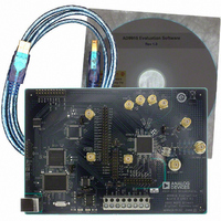
AD9910/PCBZ Analog Devices Inc, AD9910/PCBZ Datasheet - Page 29

AD9910/PCBZ
Manufacturer Part Number
AD9910/PCBZ
Description
Direct Digital Synthesis Evaluation Board
Manufacturer
Analog Devices Inc
Series
AgileRF™r
Specifications of AD9910/PCBZ
Silicon Manufacturer
Analog Devices
Application Sub Type
Direct Digital Synthesizer
Kit Application Type
Clock & Timing
Silicon Core Number
AD9910
Kit Contents
Board
Design Resources
Synchronizing Multiple AD9910 1 GSPS Direct Digital Synthesizers (CN0121)
Main Purpose
Timing, Direct Digital Synthesis (DDS)
Embedded
No
Utilized Ic / Part
AD9910
Primary Attributes
14-Bit DAC, 32-Bit Tuning Word Width
Secondary Attributes
1GHz, Graphical User Interface
Lead Free Status / RoHS Status
Lead free / RoHS Compliant
Lead Free Status / RoHS Status
Lead free / RoHS Compliant, Lead free / RoHS Compliant
Other names
Q3335404
The primary control for the DRG is the digital ramp enable bit.
When disabled, the other DRG input controls are ignored and the
internal clocks are shut down to conserve power.
The output of the DRG is a 32-bit unsigned data bus that can be
routed to any one of the three DDS signal control parameters, as
controlled by the two digital ramp destination bits in Control
Function Register 2 according to Table 11. The 32-bit output
bus is MSB-aligned with the 32-bit frequency parameter, the
16-bit phase parameter, or the 14-bit amplitude parameter, as
defined by the destination bits. When the destination is phase
or amplitude, the unused LSBs are ignored.
Table 11. Digital Ramp Destination
Digital Ramp
Destination Bits
(CFR2[21:20])
00
01
1x
1
x = Don’t care.
1
LOAD LRR AT I/O_UPDATE
DECREMENT STEP SIZE
NEGATIVE SLOPE RATE
INCREMENT STEP SIZE
DDS Signal
Control
Parameter
Frequency
Phase
Amplitude
POSITIVE SLOPE RATE
DDS CLOCK
DRHOLD
DRCTL
62
63
CONTROL
LOGIC
32
32
16
16
LOAD
Bits Assigned to
DDS Parameter
31:0
31:16
31:18
0
1
0
1
Figure 38. Digital Ramp Generator Detail
32
16
LOAD
PRESET
DIGITAL
TIMER
RAMP
Rev. C | Page 29 of 64
Q
32
32
DIGITAL RAMP ACCUMULATOR
D
R
Q
ACCUMULATOR
The ramp characteristics of the DRG are fully programmable. This
includes the upper and lower ramp limits, and independent control
of the step size and step rate for both the positive and negative slope
characteristics of the ramp. A detailed block diagram of the DRG is
shown in Figure 38.
The direction of the ramping function is controlled by the
DRCTL pin. A Logic 0 on this pin causes the DRG to ramp
with a negative slope, whereas a Logic 1 causes the DRG to
ramp with a positive slope.
The DRG also supports a hold feature controlled via the DRHOLD
pin. When this pin is set to Logic 1, the DRG is stalled at its last
state; otherwise, the DRG operates normally.
The DDS signal control parameters that are not the destination of
the DRG are taken from the active profile.
CONTROL
RESET
LOGIC
32
UPPER
LIMIT
LIMIT CONTROL
32
LOWER
LIMIT
CLEAR DIGITAL RAMP ACCUMULATOR
AUTOCLEAR DIGITAL RAMP ACC
NO-DWELL
CONTROL
32
2
NO DWELL
TO DDS
SIGNAL
CONTROL
PARAMETER
.
AD9910


