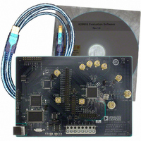
AD9910/PCBZ Analog Devices Inc, AD9910/PCBZ Datasheet - Page 58

AD9910/PCBZ
Manufacturer Part Number
AD9910/PCBZ
Description
Direct Digital Synthesis Evaluation Board
Manufacturer
Analog Devices Inc
Series
AgileRF™r
Specifications of AD9910/PCBZ
Silicon Manufacturer
Analog Devices
Application Sub Type
Direct Digital Synthesizer
Kit Application Type
Clock & Timing
Silicon Core Number
AD9910
Kit Contents
Board
Design Resources
Synchronizing Multiple AD9910 1 GSPS Direct Digital Synthesizers (CN0121)
Main Purpose
Timing, Direct Digital Synthesis (DDS)
Embedded
No
Utilized Ic / Part
AD9910
Primary Attributes
14-Bit DAC, 32-Bit Tuning Word Width
Secondary Attributes
1GHz, Graphical User Interface
Lead Free Status / RoHS Status
Lead free / RoHS Compliant
Lead Free Status / RoHS Status
Lead free / RoHS Compliant, Lead free / RoHS Compliant
Other names
Q3335404
AD9910
Bit(s)
6
5
4
3:0
Control Function Register 3 (CFR3)—Address 0x02
Four bytes are assigned to this register.
Table 20. Bit Descriptions for CFR3
Bit(s)
31:30
29:28
27
26:24
23:22
21:19
18:16
15
14
13:11
10
9
8
7:1
0
Auxiliary DAC Control Register—Address 0x03
Four bytes are assigned to this register.
Table 21. Bit Descriptions for DAC Control Register
Bit(s)
31:8
7:0
Mnemonic
Data assembler hold last
value
Sync timing validation
disable
Parallel data port enable
FM gain
Mnemonic
Open
DRV0
Open
VCO SEL
Open
I
Open
REFCLK input divider bypass
REFCLK input divider ResetB
Open
PFD reset
Open
PLL enable
N
Open
Mnemonic
Open
FSC
CP
Description
Ineffective unless CFR2[4] = 1.
0 = enables the SYNC_SMP_ERR pin to indicate (active high) detection of a synchronization
pulse sampling error.
1 = the SYNC_SMP_ERR pin is forced to a static Logic 0 condition (default).
See the Parallel Data Port Modulation Mode section for more details.
See the Parallel Data Port Modulation Mode section for more details. Default is 0000b.
Description
Controls the REFCLK_OUT pin (see Table 7 for details); default is 00b.
Selects the frequency band of the REFCLK PLL VCO (see Table 8 for details); default is 111b.
Selects the charge pump current in the REFCLK PLL (see Table 9 for details); default is 111b.
0 = input divider is selected (default).
1 = input divider is bypassed.
0 = input divider is reset.
1 = input divider operates normally (default).
0 = normal operation (default).
1 = phase detector disabled.
0 = REFCLK PLL bypassed (default).
1 = REFCLK PLL enabled.
This 7-bit number is the divide modulus of the REFCLK PLL feedback divider; default is
0000000b.
Description
This 8-bit number controls the full-scale output current of the main DAC (see the Auxiliary
DAC section); default is 0x7F.
0 = the data assembler of the parallel data port internally forces zeros on the data path
and ignores the signals on the D[15:0] and F[1:0] pins while the TxENABLE pin is Logic 0
(default). This implies that the destination of the data at the parallel data port is
amplitude when TxENABLE is Logic 0.
1 = the data assembler of the parallel data port internally forces the last value received
on the D[15:0] and F[1:0] pins while the TxENABLE pin is Logic 1.
0 = disables parallel data port modulation functionality (default).
1 = enables parallel data port modulation functionality.
Rev. C | Page 58 of 64


