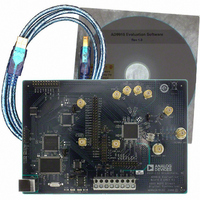
AD9910/PCBZ Analog Devices Inc, AD9910/PCBZ Datasheet - Page 22

AD9910/PCBZ
Manufacturer Part Number
AD9910/PCBZ
Description
Direct Digital Synthesis Evaluation Board
Manufacturer
Analog Devices Inc
Series
AgileRF™r
Specifications of AD9910/PCBZ
Silicon Manufacturer
Analog Devices
Application Sub Type
Direct Digital Synthesizer
Kit Application Type
Clock & Timing
Silicon Core Number
AD9910
Kit Contents
Board
Design Resources
Synchronizing Multiple AD9910 1 GSPS Direct Digital Synthesizers (CN0121)
Main Purpose
Timing, Direct Digital Synthesis (DDS)
Embedded
No
Utilized Ic / Part
AD9910
Primary Attributes
14-Bit DAC, 32-Bit Tuning Word Width
Secondary Attributes
1GHz, Graphical User Interface
Lead Free Status / RoHS Status
Lead free / RoHS Compliant
Lead Free Status / RoHS Status
Lead free / RoHS Compliant, Lead free / RoHS Compliant
Other names
Q3335404
AD9910
MODE PRIORITY
The three different modulation modes generate frequency,
phase, and/or amplitude data destined for the DDS signal
control parameters. In addition, the OSK function generates
amplitude data destined for the DDS. Each of these functions is
independently invoked using the appropriate control bit via the
serial I/O port.
The ability to activate each of these functions independently
makes it possible to have multiple data sources attempting to
Table 5. Data Source Priority
Highest
Priority
Lowest
Priority
Priority
Data Source
RAM
DRG
Parallel data
port and FTW
register
FTW register
FTW in active
single tone
profile register
FTW in active
single tone
profile register
FTW in active
single tone
profile register
Frequency
Conditions
RAM enabled and
data destination is
frequency
DRG enabled and
data destination is
frequency
Parallel data port
enabled and data
destination is
frequency
RAM enabled and
data destination is
phase, amplitude,
or polar
DRG enabled and
data destination is
phase or amplitude
Parallel data port
enabled and data
destination is
phase, amplitude,
or polar
None
Data Source
RAM
DRG
Parallel data port
Parallel data port
concatenated with
the POW register
LSBs
POW register
POW in active
single tone profile
register
POW in active
single tone profile
register
POW in active
single tone profile
register
DDS Signal Control Parameters
Rev. C | Page 22 of 64
Phase
drive the same DDS signal control parameter. To avoid contention,
the AD9910 has a built-in priority system. Table 5 summarizes
the priority for each of the DDS signal control parameters. The
rows of Table 5 list data sources for a particular DDS signal con-
trol parameter in descending order of precedence. For example,
if both the RAM and the parallel port are enabled and both are
programmed for frequency as the destination, then the DDS
frequency parameter is driven by the RAM and not the parallel
data port.
Conditions
RAM enabled and
data destination is
phase or polar
DRG enabled and
data destination is
phase
Parallel data port
enabled and data
destination is
phase
Parallel data port
enabled and data
destination is polar
RAM enabled and
destination is
frequency or
amplitude
DRG enabled and
data destination is
frequency or
amplitude
Parallel data port
enabled and data
destination is
frequency or
amplitude
None
Data Source
OSK generator
ASF register
RAM
DRG
Parallel data port
Parallel data port
concatenated with
the ASF register
LSBs
ASF in active single
tone profile
register
No amplitude
scaling
Amplitude
Conditions
OSK enabled (auto
mode)
OSK enabled
(manual mode)
RAM enabled and
data destination is
amplitude or polar
DRG enabled and
data destination is
amplitude
Parallel data port
enabled and data
destination is
amplitude
Parallel data port
enabled and data
destination is
polar
Enable amplitude
scale from single
tone profiles bit
(CFR2[24]) set
None


