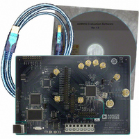
AD9910/PCBZ Analog Devices Inc, AD9910/PCBZ Datasheet - Page 39

AD9910/PCBZ
Manufacturer Part Number
AD9910/PCBZ
Description
Direct Digital Synthesis Evaluation Board
Manufacturer
Analog Devices Inc
Series
AgileRF™r
Specifications of AD9910/PCBZ
Silicon Manufacturer
Analog Devices
Application Sub Type
Direct Digital Synthesizer
Kit Application Type
Clock & Timing
Silicon Core Number
AD9910
Kit Contents
Board
Design Resources
Synchronizing Multiple AD9910 1 GSPS Direct Digital Synthesizers (CN0121)
Main Purpose
Timing, Direct Digital Synthesis (DDS)
Embedded
No
Utilized Ic / Part
AD9910
Primary Attributes
14-Bit DAC, 32-Bit Tuning Word Width
Secondary Attributes
1GHz, Graphical User Interface
Lead Free Status / RoHS Status
Lead free / RoHS Compliant
Lead Free Status / RoHS Status
Lead free / RoHS Compliant, Lead free / RoHS Compliant
Other names
Q3335404
If the PROFILE0 pin changes states before the state machine
reaches the programmed start or end address, the internal timer
is restarted and the direction of the address counter is reversed.
Figure 46 is a graphic representation of the bidirectional ramp
mode. It shows the action of the state machine in response to
the PROFILE0 pin and the response of the RAM_SWP_OVR pin.
The RAM_SWP_OVR pin switches to Logic 1 when the state
machine reaches the waveform end address. It remains Logic 1
until the state machine reaches the waveform start address and
the PROFILE0 pin transitions from Logic 0 to Logic 1.
The circled numbers in Figure 46 indicate specific events as
follows:
Event 1—An I/O update or profile change activates the RAM
bidirectional ramp mode. The state machine initializes to the
waveform start address, and the RAM_SWP_OVR pin is set to
Logic 0.
Event 2—Pin PROFILE0 switches to Logic 1. The state machine
begins incrementing the RAM address counter.
Event 3—Pin PROFILE0 remains at Logic 1 long enough for the
state machine to reach the waveform end address. The RAM_
SWP_OVR pin switches to Logic 1 accordingly.
Event 4—Pin PROFILE0 switches to Logic 0. The state machine
begins decrementing the RAM address counter. The RAM_
SWP_OVR pin remains at Logic 1.
Event 5—Pin PROFILE0 switches to Logic 1. The state machine
resets its internal timer and reverses the direction of the RAM
address counter (that is, it starts to increment). There is no
change of the RAM_SWP_OVR state because the waveform
start address has not yet been reached.
RAM_SWP_OVER
RAM ADRESS
I/O_UPDATE
PROFILE0
1
WAVEFORM END ADDRESS
2
WAVEFORM START ADDRESS
M DDS CLOCK CYCLES
1
Figure 46. Bidirectional Ramp Timing Diagram
Δ
t
3
Rev. C | Page 39 of 64
4
Δ
t
Event 6—Pin PROFILE0 switches to Logic 0. The state machine
resets its internal timer and again reverses the direction of the RAM
address counter. The RAM_SWP_OVR state does not change.
Event 7—Pin PROFILE0 remains at Logic 0 long enough for the
state machine to reach the waveform start address. There is no
change in the RAM_SWP_OVR state.
Event 8—Pin PROFILE0 switches to Logic 1. The state machine
resets its internal timer and begins incrementing the RAM
address counter. The RAM_SWP_OVR pin switches to Logic 0
because both the waveform start address was reached and the
PROFILE0 pin transitioned from Logic 0 to Logic 1.
RAM Continuous Bidirectional Ramp Mode
In continuous bidirectional ramp mode, upon assertion of an
I/O update or a change of profile, the RAM begins operating
as a waveform generator using the parameters programmed
into the RAM profile designated by the PROFILEx pins. Data is
extracted from RAM over the specified address range and at the
specified rate contained in the waveform start address, waveform
end address, and address ramp rate values of the selected RAM
profile. The data is delivered to the specified DDS signal control
parameter(s) based on the RAM playback destination bits. The
no-dwell high bit is ignored in this mode.
With the continuous bidirectional ramp mode activated via an
I/O update or profile change, the internal state machine begins
extracting data from the RAM at the waveform start address and
incrementing the address counter until it reaches the waveform
end address. At this point, the state machine automatically reverses
the direction of the address counter and begins decrementing
through the address range. Whenever one of the terminal
addresses is reached, the state machine reverses the address
counter; the process continues indefinitely.
5
6
7
8
AD9910


