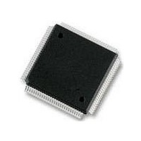
MC9S12DT256MPVE Freescale Semiconductor, MC9S12DT256MPVE Datasheet - Page 966

MC9S12DT256MPVE
Manufacturer Part Number
MC9S12DT256MPVE
Description
IC MCU 256K FLASH 25MHZ 112-LQFP
Manufacturer
Freescale Semiconductor
Series
HCS12r
Datasheet
1.S912XDG128F2MAL.pdf
(1348 pages)
Specifications of MC9S12DT256MPVE
Core Processor
HCS12
Core Size
16-Bit
Speed
25MHz
Connectivity
CAN, I²C, SCI, SPI
Peripherals
PWM, WDT
Number Of I /o
91
Program Memory Size
256KB (256K x 8)
Program Memory Type
FLASH
Eeprom Size
4K x 8
Ram Size
12K x 8
Voltage - Supply (vcc/vdd)
2.35 V ~ 5.25 V
Data Converters
A/D 8x10b
Oscillator Type
Internal
Operating Temperature
-40°C ~ 125°C
Package / Case
112-LQFP
Processor Series
S12D
Core
HCS12
Data Bus Width
16 bit
Data Ram Size
12 KB
Interface Type
CAN/I2C/SCI/SPI
Maximum Clock Frequency
25 MHz
Number Of Programmable I/os
91
Number Of Timers
1
Operating Supply Voltage
5 V to 2.5 V
Maximum Operating Temperature
+ 125 C
Mounting Style
SMD/SMT
3rd Party Development Tools
EWHCS12
Development Tools By Supplier
M68KIT912DP256
Minimum Operating Temperature
- 40 C
On-chip Adc
2 (8-ch x 10-bit)
No. Of I/o's
91
Eeprom Memory Size
4KB
Ram Memory Size
12KB
Cpu Speed
25MHz
No. Of Timers
1
No. Of Pwm Channels
8
Digital Ic Case Style
LQFP
Rohs Compliant
Yes
Lead Free Status / RoHS Status
Lead free / RoHS Compliant
Available stocks
Company
Part Number
Manufacturer
Quantity
Price
Company:
Part Number:
MC9S12DT256MPVE
Manufacturer:
Freescale Semiconductor
Quantity:
10 000
- Current page: 966 of 1348
- Download datasheet (8Mb)
Chapter 23 DQ256 Port Integration Module (S12XDQ256PIMV2)
open-drain output pins. The CAN4 pins can be re-routed. Refer to
Register
Port J pins can be used with the routed CAN0 modules. Refer to
Register
Port J offers 7 I/O pins with edge triggered interrupt capability
23.0.7.12 Port AD0
This port is associated with the ATD0. Port AD0 pins PAD07–PAD00 can be used for either general
purpose I/O, or with the ATD0 subsystem.
23.0.7.13 Port AD1
This port is associated with the ATD1. Port AD1 pins PAD23–PAD8 can be used for either general
purpose I/O, or with the ATD1 subsystem.
23.0.8
Ports P, H and J offer pin interrupt capability. The interrupt enable as well as the sensitivity to rising or
falling edges can be individually configured on per-pin basis. All bits/pins in a port share the same
interrupt vector. Interrupts can be used with the pins configured as inputs or outputs.
An interrupt is generated when a bit in the port interrupt flag register and its corresponding port interrupt
enable bit are both set. The pin interrupt feature is also capable to wake up the CPU when it is in STOP or
WAIT mode.
A digital filter on each pin prevents pulses
interrupt. The minimum time varies over process conditions, temperature and voltage
Table
968
23-69).
(MODRR)”.
(MODRR)”.
Pin Interrupts
PJ[5,4,2] are not available in 112-pin packages. PJ[5,4,2,1,0] are not
available in 80-pin packages.
PAD[23:16] are not available in 112-pin packages. PAD[23:8] are not
available in 80-pin packages.
MC9S12XDP512 Data Sheet, Rev. 2.21
(Figure
NOTE
NOTE
23-78) shorter than a specified time from generating an
(Section 23.0.8, “Pin
Section 23.0.5.37, “Module Routing
Section 23.0.5.37, “Module Routing
Freescale Semiconductor
Interrupts”).
(Figure 23-77
and
Related parts for MC9S12DT256MPVE
Image
Part Number
Description
Manufacturer
Datasheet
Request
R
Part Number:
Description:
Manufacturer:
Freescale Semiconductor, Inc
Datasheet:
Part Number:
Description:
Manufacturer:
Freescale Semiconductor, Inc
Datasheet:
Part Number:
Description:
Manufacturer:
Freescale Semiconductor, Inc
Datasheet:
Part Number:
Description:
Manufacturer:
Freescale Semiconductor, Inc
Datasheet:
Part Number:
Description:
Manufacturer:
Freescale Semiconductor, Inc
Datasheet:
Part Number:
Description:
Manufacturer:
Freescale Semiconductor, Inc
Datasheet:
Part Number:
Description:
Manufacturer:
Freescale Semiconductor, Inc
Datasheet:
Part Number:
Description:
Manufacturer:
Freescale Semiconductor, Inc
Datasheet:
Part Number:
Description:
Manufacturer:
Freescale Semiconductor, Inc
Datasheet:
Part Number:
Description:
Manufacturer:
Freescale Semiconductor, Inc
Datasheet:
Part Number:
Description:
Manufacturer:
Freescale Semiconductor, Inc
Datasheet:
Part Number:
Description:
Manufacturer:
Freescale Semiconductor, Inc
Datasheet:
Part Number:
Description:
Manufacturer:
Freescale Semiconductor, Inc
Datasheet:
Part Number:
Description:
Manufacturer:
Freescale Semiconductor, Inc
Datasheet:
Part Number:
Description:
Manufacturer:
Freescale Semiconductor, Inc
Datasheet:


