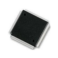
MC9S12DT256MPVE Freescale Semiconductor, MC9S12DT256MPVE Datasheet - Page 387

MC9S12DT256MPVE
Manufacturer Part Number
MC9S12DT256MPVE
Description
IC MCU 256K FLASH 25MHZ 112-LQFP
Manufacturer
Freescale Semiconductor
Series
HCS12r
Datasheet
1.S912XDG128F2MAL.pdf
(1348 pages)
Specifications of MC9S12DT256MPVE
Core Processor
HCS12
Core Size
16-Bit
Speed
25MHz
Connectivity
CAN, I²C, SCI, SPI
Peripherals
PWM, WDT
Number Of I /o
91
Program Memory Size
256KB (256K x 8)
Program Memory Type
FLASH
Eeprom Size
4K x 8
Ram Size
12K x 8
Voltage - Supply (vcc/vdd)
2.35 V ~ 5.25 V
Data Converters
A/D 8x10b
Oscillator Type
Internal
Operating Temperature
-40°C ~ 125°C
Package / Case
112-LQFP
Processor Series
S12D
Core
HCS12
Data Bus Width
16 bit
Data Ram Size
12 KB
Interface Type
CAN/I2C/SCI/SPI
Maximum Clock Frequency
25 MHz
Number Of Programmable I/os
91
Number Of Timers
1
Operating Supply Voltage
5 V to 2.5 V
Maximum Operating Temperature
+ 125 C
Mounting Style
SMD/SMT
3rd Party Development Tools
EWHCS12
Development Tools By Supplier
M68KIT912DP256
Minimum Operating Temperature
- 40 C
On-chip Adc
2 (8-ch x 10-bit)
No. Of I/o's
91
Eeprom Memory Size
4KB
Ram Memory Size
12KB
Cpu Speed
25MHz
No. Of Timers
1
No. Of Pwm Channels
8
Digital Ic Case Style
LQFP
Rohs Compliant
Yes
Lead Free Status / RoHS Status
Lead free / RoHS Compliant
Available stocks
Company
Part Number
Manufacturer
Quantity
Price
Company:
Part Number:
MC9S12DT256MPVE
Manufacturer:
Freescale Semiconductor
Quantity:
10 000
- Current page: 387 of 1348
- Download datasheet (8Mb)
To calculate the output frequency in left aligned output mode for a particular channel, take the selected
clock source frequency for the channel (A, B, SA, or SB) and divide it by the value in the period register
for that channel.
As an example of a left aligned output, consider the following case:
The output waveform generated is shown in
Freescale Semiconductor
•
•
•
Duty Cycle = [PWMDTYx / PWMPERx] * 100%
PWMx Frequency = Clock (A, B, SA, or SB) / PWMPERx
PWMx Duty Cycle (high time as a% of period):
— Polarity = 0 (PPOLx = 0)
Duty Cycle = [(PWMPERx-PWMDTYx)/PWMPERx] * 100%
— Polarity = 1 (PPOLx = 1)
Clock Source = E, where E = 10 MHz (100 ns period)
PWMx Frequency = 10 MHz/4 = 2.5 MHz
PWMx Period = 400 ns
PWMx Duty Cycle = 3/4 *100% = 75%
PPOLx = 0
PWMPERx = 4
PWMDTYx = 1
Changing the PWM output mode from left aligned to center aligned output
(or vice versa) while channels are operating can cause irregularities in the
PWM output. It is recommended to program the output mode before
enabling the PWM channel.
PPOLx = 0
PPOLx = 1
Figure 8-20. PWM Left Aligned Output Waveform
MC9S12XDP512 Data Sheet, Rev. 2.21
PWMDTYx
Figure
NOTE
Period = PWMPERx
8-21.
Chapter 8 Pulse-Width Modulator (S12PWM8B8CV1)
387
Related parts for MC9S12DT256MPVE
Image
Part Number
Description
Manufacturer
Datasheet
Request
R
Part Number:
Description:
Manufacturer:
Freescale Semiconductor, Inc
Datasheet:
Part Number:
Description:
Manufacturer:
Freescale Semiconductor, Inc
Datasheet:
Part Number:
Description:
Manufacturer:
Freescale Semiconductor, Inc
Datasheet:
Part Number:
Description:
Manufacturer:
Freescale Semiconductor, Inc
Datasheet:
Part Number:
Description:
Manufacturer:
Freescale Semiconductor, Inc
Datasheet:
Part Number:
Description:
Manufacturer:
Freescale Semiconductor, Inc
Datasheet:
Part Number:
Description:
Manufacturer:
Freescale Semiconductor, Inc
Datasheet:
Part Number:
Description:
Manufacturer:
Freescale Semiconductor, Inc
Datasheet:
Part Number:
Description:
Manufacturer:
Freescale Semiconductor, Inc
Datasheet:
Part Number:
Description:
Manufacturer:
Freescale Semiconductor, Inc
Datasheet:
Part Number:
Description:
Manufacturer:
Freescale Semiconductor, Inc
Datasheet:
Part Number:
Description:
Manufacturer:
Freescale Semiconductor, Inc
Datasheet:
Part Number:
Description:
Manufacturer:
Freescale Semiconductor, Inc
Datasheet:
Part Number:
Description:
Manufacturer:
Freescale Semiconductor, Inc
Datasheet:
Part Number:
Description:
Manufacturer:
Freescale Semiconductor, Inc
Datasheet:


