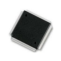
MC9S12DT256MPVE Freescale Semiconductor, MC9S12DT256MPVE Datasheet - Page 1009

MC9S12DT256MPVE
Manufacturer Part Number
MC9S12DT256MPVE
Description
IC MCU 256K FLASH 25MHZ 112-LQFP
Manufacturer
Freescale Semiconductor
Series
HCS12r
Datasheet
1.S912XDG128F2MAL.pdf
(1348 pages)
Specifications of MC9S12DT256MPVE
Core Processor
HCS12
Core Size
16-Bit
Speed
25MHz
Connectivity
CAN, I²C, SCI, SPI
Peripherals
PWM, WDT
Number Of I /o
91
Program Memory Size
256KB (256K x 8)
Program Memory Type
FLASH
Eeprom Size
4K x 8
Ram Size
12K x 8
Voltage - Supply (vcc/vdd)
2.35 V ~ 5.25 V
Data Converters
A/D 8x10b
Oscillator Type
Internal
Operating Temperature
-40°C ~ 125°C
Package / Case
112-LQFP
Processor Series
S12D
Core
HCS12
Data Bus Width
16 bit
Data Ram Size
12 KB
Interface Type
CAN/I2C/SCI/SPI
Maximum Clock Frequency
25 MHz
Number Of Programmable I/os
91
Number Of Timers
1
Operating Supply Voltage
5 V to 2.5 V
Maximum Operating Temperature
+ 125 C
Mounting Style
SMD/SMT
3rd Party Development Tools
EWHCS12
Development Tools By Supplier
M68KIT912DP256
Minimum Operating Temperature
- 40 C
On-chip Adc
2 (8-ch x 10-bit)
No. Of I/o's
91
Eeprom Memory Size
4KB
Ram Memory Size
12KB
Cpu Speed
25MHz
No. Of Timers
1
No. Of Pwm Channels
8
Digital Ic Case Style
LQFP
Rohs Compliant
Yes
Lead Free Status / RoHS Status
Lead free / RoHS Compliant
Available stocks
Company
Part Number
Manufacturer
Quantity
Price
Company:
Part Number:
MC9S12DT256MPVE
Manufacturer:
Freescale Semiconductor
Quantity:
10 000
- Current page: 1009 of 1348
- Download datasheet (8Mb)
WOMM[7:0]
Reset
This register configures the output pins as wired-OR. If enabled the output is driven active low only
(open-drain). A logic level of “1” is not driven. It applies also to the CAN outputs and allows a
multipoint connection of several serial modules. This bit has no influence on pins used as inputs.
Field
24.0.5.33 Module Routing Register (MODRR)
1. Register implemented, function disabled: Written values can be read back.
Read: Anytime.
Write: Anytime.
This register configures the re-routing of CAN0, CAN4, SPI0, SPI1 on alternative ports.
7–0
W
R
Module
Wired-OR Mode Port M
0 Output buffers operate as push-pull outputs.
1 Output buffers operate as open-drain outputs.
CAN0
CAN4
SPI0
SPI1
7
0
0
= Unimplemented or Reserved
6
x
x
x
x
x
x
x
x
x
x
x
x
MODRR6
5
0
1
0
x
x
x
x
x
x
x
x
x
x
6
Figure 24-35. Module Routing Register (MODRR)
1
4
0
1
x
x
x
x
x
x
x
x
x
x
MODRR
Table 24-34. Module Routing Summary
Table 24-33. WOMM Field Descriptions
MODRR5
3
x
x
x
x
0
0
1
1
x
x
x
x
5
0
2
x
x
x
x
0
1
0
1
x
x
x
x
1
0
0
1
1
x
x
x
x
x
x
x
x
MODRR4
0
0
1
0
1
x
x
x
x
x
x
x
x
0
4
Description
MISO
PM2
PS4
PP0
PH0
RXCAN
MODRR3
PM0
PM2
PM4
PM4
PM6
PJ6
PJ6
3
0
MOSI
PM4
PH1
PS5
PP1
Related Pins
Reserved
MODRR2
0
2
SCK
PM5
PS6
PP2
PH2
TXCAN
PM1
PM3
PM5
PM5
PM7
PJ7
PJ7
MODRR1
1
0
PM3
PH3
PS7
PP3
SS
MODRR0
0
0
Related parts for MC9S12DT256MPVE
Image
Part Number
Description
Manufacturer
Datasheet
Request
R
Part Number:
Description:
Manufacturer:
Freescale Semiconductor, Inc
Datasheet:
Part Number:
Description:
Manufacturer:
Freescale Semiconductor, Inc
Datasheet:
Part Number:
Description:
Manufacturer:
Freescale Semiconductor, Inc
Datasheet:
Part Number:
Description:
Manufacturer:
Freescale Semiconductor, Inc
Datasheet:
Part Number:
Description:
Manufacturer:
Freescale Semiconductor, Inc
Datasheet:
Part Number:
Description:
Manufacturer:
Freescale Semiconductor, Inc
Datasheet:
Part Number:
Description:
Manufacturer:
Freescale Semiconductor, Inc
Datasheet:
Part Number:
Description:
Manufacturer:
Freescale Semiconductor, Inc
Datasheet:
Part Number:
Description:
Manufacturer:
Freescale Semiconductor, Inc
Datasheet:
Part Number:
Description:
Manufacturer:
Freescale Semiconductor, Inc
Datasheet:
Part Number:
Description:
Manufacturer:
Freescale Semiconductor, Inc
Datasheet:
Part Number:
Description:
Manufacturer:
Freescale Semiconductor, Inc
Datasheet:
Part Number:
Description:
Manufacturer:
Freescale Semiconductor, Inc
Datasheet:
Part Number:
Description:
Manufacturer:
Freescale Semiconductor, Inc
Datasheet:
Part Number:
Description:
Manufacturer:
Freescale Semiconductor, Inc
Datasheet:


