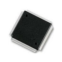
MC9S12DT256MPVE Freescale Semiconductor, MC9S12DT256MPVE Datasheet - Page 963

MC9S12DT256MPVE
Manufacturer Part Number
MC9S12DT256MPVE
Description
IC MCU 256K FLASH 25MHZ 112-LQFP
Manufacturer
Freescale Semiconductor
Series
HCS12r
Datasheet
1.S912XDG128F2MAL.pdf
(1348 pages)
Specifications of MC9S12DT256MPVE
Core Processor
HCS12
Core Size
16-Bit
Speed
25MHz
Connectivity
CAN, I²C, SCI, SPI
Peripherals
PWM, WDT
Number Of I /o
91
Program Memory Size
256KB (256K x 8)
Program Memory Type
FLASH
Eeprom Size
4K x 8
Ram Size
12K x 8
Voltage - Supply (vcc/vdd)
2.35 V ~ 5.25 V
Data Converters
A/D 8x10b
Oscillator Type
Internal
Operating Temperature
-40°C ~ 125°C
Package / Case
112-LQFP
Processor Series
S12D
Core
HCS12
Data Bus Width
16 bit
Data Ram Size
12 KB
Interface Type
CAN/I2C/SCI/SPI
Maximum Clock Frequency
25 MHz
Number Of Programmable I/os
91
Number Of Timers
1
Operating Supply Voltage
5 V to 2.5 V
Maximum Operating Temperature
+ 125 C
Mounting Style
SMD/SMT
3rd Party Development Tools
EWHCS12
Development Tools By Supplier
M68KIT912DP256
Minimum Operating Temperature
- 40 C
On-chip Adc
2 (8-ch x 10-bit)
No. Of I/o's
91
Eeprom Memory Size
4KB
Ram Memory Size
12KB
Cpu Speed
25MHz
No. Of Timers
1
No. Of Pwm Channels
8
Digital Ic Case Style
LQFP
Rohs Compliant
Yes
Lead Free Status / RoHS Status
Lead free / RoHS Compliant
Available stocks
Company
Part Number
Manufacturer
Quantity
Price
Company:
Part Number:
MC9S12DT256MPVE
Manufacturer:
Freescale Semiconductor
Quantity:
10 000
- Current page: 963 of 1348
- Download datasheet (8Mb)
23.0.6.10 Module Routing Register
This register supports the re-routing of the CAN0, CAN4, SPI0, SPI1, and SPI2 pins to alternative
ports. This allows a software re-configuration of the pinouts of the different package options with
respect to above peripherals.
23.0.7
23.0.7.1
The BKGD pin is associated with the S12X_BDM and S12X_EBI modules. During reset, the
BKGD pin is used as MODC input.
23.0.7.2
Port A pins PA[7:0] and Port B pins PB[7:0] can be used for either general-purpose I/O, or, in 144-
pin packages, also with the external bus interface. In this case port A and port B are associated with
the external address bus outputs ADDR15–ADDR8 and ADDR7–ADDR0, respectively. PB0 is the
ADDR0 or UDS output.
23.0.7.3
Port C pins PC[7:0] and port D pins PD[7:0] can be used for either general-purpose I/O, or, in 144-
pin packages, also with the external bus interface. In this case port C and port D are associated with
the external data bus inputs/outputs DATA15–DATA8 and DATA7–DATA0, respectively.
These pins are configured for reduced input threshold in certain operating modes (refer to
S12X_EBI section).
of Modules
Number
5
4
3
2
1
Ports
BKGD Pin
Port A and B
Port C and D
The purpose of the module routing register is to provide maximum
flexibility for derivatives with a lower number of MSCAN and SPI
modules.
Port C and D are neither available in 112-pin nor in 80-pin packages.
CAN0
Table 23-68. Module Implementations on Derivatives
yes
yes
yes
yes
yes
CAN1
yes
yes
yes
—
—
MSCAN Modules
CAN2
yes
yes
—
—
—
NOTE
NOTE
CAN3
yes
—
—
—
—
CAN4
yes
yes
yes
yes
—
SPI0
yes
yes
yes
—
—
SPI Modules
SPI1
yes
yes
—
—
—
SPI2
yes
—
—
—
—
Related parts for MC9S12DT256MPVE
Image
Part Number
Description
Manufacturer
Datasheet
Request
R
Part Number:
Description:
Manufacturer:
Freescale Semiconductor, Inc
Datasheet:
Part Number:
Description:
Manufacturer:
Freescale Semiconductor, Inc
Datasheet:
Part Number:
Description:
Manufacturer:
Freescale Semiconductor, Inc
Datasheet:
Part Number:
Description:
Manufacturer:
Freescale Semiconductor, Inc
Datasheet:
Part Number:
Description:
Manufacturer:
Freescale Semiconductor, Inc
Datasheet:
Part Number:
Description:
Manufacturer:
Freescale Semiconductor, Inc
Datasheet:
Part Number:
Description:
Manufacturer:
Freescale Semiconductor, Inc
Datasheet:
Part Number:
Description:
Manufacturer:
Freescale Semiconductor, Inc
Datasheet:
Part Number:
Description:
Manufacturer:
Freescale Semiconductor, Inc
Datasheet:
Part Number:
Description:
Manufacturer:
Freescale Semiconductor, Inc
Datasheet:
Part Number:
Description:
Manufacturer:
Freescale Semiconductor, Inc
Datasheet:
Part Number:
Description:
Manufacturer:
Freescale Semiconductor, Inc
Datasheet:
Part Number:
Description:
Manufacturer:
Freescale Semiconductor, Inc
Datasheet:
Part Number:
Description:
Manufacturer:
Freescale Semiconductor, Inc
Datasheet:
Part Number:
Description:
Manufacturer:
Freescale Semiconductor, Inc
Datasheet:


