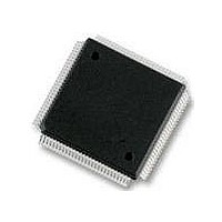
MC9S12DT256MPVE Freescale Semiconductor, MC9S12DT256MPVE Datasheet - Page 176

MC9S12DT256MPVE
Manufacturer Part Number
MC9S12DT256MPVE
Description
IC MCU 256K FLASH 25MHZ 112-LQFP
Manufacturer
Freescale Semiconductor
Series
HCS12r
Datasheet
1.S912XDG128F2MAL.pdf
(1348 pages)
Specifications of MC9S12DT256MPVE
Core Processor
HCS12
Core Size
16-Bit
Speed
25MHz
Connectivity
CAN, I²C, SCI, SPI
Peripherals
PWM, WDT
Number Of I /o
91
Program Memory Size
256KB (256K x 8)
Program Memory Type
FLASH
Eeprom Size
4K x 8
Ram Size
12K x 8
Voltage - Supply (vcc/vdd)
2.35 V ~ 5.25 V
Data Converters
A/D 8x10b
Oscillator Type
Internal
Operating Temperature
-40°C ~ 125°C
Package / Case
112-LQFP
Processor Series
S12D
Core
HCS12
Data Bus Width
16 bit
Data Ram Size
12 KB
Interface Type
CAN/I2C/SCI/SPI
Maximum Clock Frequency
25 MHz
Number Of Programmable I/os
91
Number Of Timers
1
Operating Supply Voltage
5 V to 2.5 V
Maximum Operating Temperature
+ 125 C
Mounting Style
SMD/SMT
3rd Party Development Tools
EWHCS12
Development Tools By Supplier
M68KIT912DP256
Minimum Operating Temperature
- 40 C
On-chip Adc
2 (8-ch x 10-bit)
No. Of I/o's
91
Eeprom Memory Size
4KB
Ram Memory Size
12KB
Cpu Speed
25MHz
No. Of Timers
1
No. Of Pwm Channels
8
Digital Ic Case Style
LQFP
Rohs Compliant
Yes
Lead Free Status / RoHS Status
Lead free / RoHS Compliant
Available stocks
Company
Part Number
Manufacturer
Quantity
Price
Company:
Part Number:
MC9S12DT256MPVE
Manufacturer:
Freescale Semiconductor
Quantity:
10 000
- Current page: 176 of 1348
- Download datasheet (8Mb)
Chapter 5 Analog-to-Digital Converter (S12ATD10B8CV2)
5.3.2.8
Read: Anytime, returns unpredictable values
Write: Anytime in special modes, unimplemented in normal modes
5.3.2.9
This register contains the SC bit used to enable special channel conversions.
Read: Anytime, returns unpredictable values for Bit7 and Bit6
Write: Anytime
176
Reset
Reset
Field
SC
0
W
W
R
R
Special Channel Conversion Bit — If this bit is set, then special channel conversion can be selected using CC,
CB and CA of ATDCTL5.
0 Special channel conversions disabled
1 Special channel conversions enabled
Note: Always write remaining bits of ATDTEST1 (Bit7 to Bit1) zero when writing SC bit. Not doing so might result
Reserved Register (ATDTEST0)
ATD Test Register 1 (ATDTEST1)
U
U
1
0
7
7
Writing to this register when in special modes can alter functionality.
SC
1
1
1
1
1
in unpredictable ATD behavior.
= Unimplemented or Reserved
= Unimplemented or Reserved
U
U
0
0
6
6
CC
Figure 5-11. ATD Test Register 1 (ATDTEST1)
Figure 5-10. Reserved Register (ATDTEST0)
0
1
1
1
1
Table 5-19. Special Channel Select Coding
Table 5-18. ATDTEST1 Field Descriptions
Table 5-19
MC9S12XDP512 Data Sheet, Rev. 2.21
U
0
0
0
5
5
lists the coding.
CB
X
0
0
1
1
NOTE
U
0
0
0
4
4
Description
CA
X
0
1
0
1
U
0
0
0
3
3
Analog Input Channel
(V
U
0
0
0
2
2
Reserved
Reserved
RH
+V
V
V
RH
RL
RL
) / 2
Freescale Semiconductor
U
0
0
0
1
1
SC
U
0
0
0
0
Related parts for MC9S12DT256MPVE
Image
Part Number
Description
Manufacturer
Datasheet
Request
R
Part Number:
Description:
Manufacturer:
Freescale Semiconductor, Inc
Datasheet:
Part Number:
Description:
Manufacturer:
Freescale Semiconductor, Inc
Datasheet:
Part Number:
Description:
Manufacturer:
Freescale Semiconductor, Inc
Datasheet:
Part Number:
Description:
Manufacturer:
Freescale Semiconductor, Inc
Datasheet:
Part Number:
Description:
Manufacturer:
Freescale Semiconductor, Inc
Datasheet:
Part Number:
Description:
Manufacturer:
Freescale Semiconductor, Inc
Datasheet:
Part Number:
Description:
Manufacturer:
Freescale Semiconductor, Inc
Datasheet:
Part Number:
Description:
Manufacturer:
Freescale Semiconductor, Inc
Datasheet:
Part Number:
Description:
Manufacturer:
Freescale Semiconductor, Inc
Datasheet:
Part Number:
Description:
Manufacturer:
Freescale Semiconductor, Inc
Datasheet:
Part Number:
Description:
Manufacturer:
Freescale Semiconductor, Inc
Datasheet:
Part Number:
Description:
Manufacturer:
Freescale Semiconductor, Inc
Datasheet:
Part Number:
Description:
Manufacturer:
Freescale Semiconductor, Inc
Datasheet:
Part Number:
Description:
Manufacturer:
Freescale Semiconductor, Inc
Datasheet:
Part Number:
Description:
Manufacturer:
Freescale Semiconductor, Inc
Datasheet:


