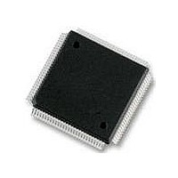
MC9S12DT256MPVE Freescale Semiconductor, MC9S12DT256MPVE Datasheet - Page 378

MC9S12DT256MPVE
Manufacturer Part Number
MC9S12DT256MPVE
Description
IC MCU 256K FLASH 25MHZ 112-LQFP
Manufacturer
Freescale Semiconductor
Series
HCS12r
Datasheet
1.S912XDG128F2MAL.pdf
(1348 pages)
Specifications of MC9S12DT256MPVE
Core Processor
HCS12
Core Size
16-Bit
Speed
25MHz
Connectivity
CAN, I²C, SCI, SPI
Peripherals
PWM, WDT
Number Of I /o
91
Program Memory Size
256KB (256K x 8)
Program Memory Type
FLASH
Eeprom Size
4K x 8
Ram Size
12K x 8
Voltage - Supply (vcc/vdd)
2.35 V ~ 5.25 V
Data Converters
A/D 8x10b
Oscillator Type
Internal
Operating Temperature
-40°C ~ 125°C
Package / Case
112-LQFP
Processor Series
S12D
Core
HCS12
Data Bus Width
16 bit
Data Ram Size
12 KB
Interface Type
CAN/I2C/SCI/SPI
Maximum Clock Frequency
25 MHz
Number Of Programmable I/os
91
Number Of Timers
1
Operating Supply Voltage
5 V to 2.5 V
Maximum Operating Temperature
+ 125 C
Mounting Style
SMD/SMT
3rd Party Development Tools
EWHCS12
Development Tools By Supplier
M68KIT912DP256
Minimum Operating Temperature
- 40 C
On-chip Adc
2 (8-ch x 10-bit)
No. Of I/o's
91
Eeprom Memory Size
4KB
Ram Memory Size
12KB
Cpu Speed
25MHz
No. Of Timers
1
No. Of Pwm Channels
8
Digital Ic Case Style
LQFP
Rohs Compliant
Yes
Lead Free Status / RoHS Status
Lead free / RoHS Compliant
Available stocks
Company
Part Number
Manufacturer
Quantity
Price
Company:
Part Number:
MC9S12DT256MPVE
Manufacturer:
Freescale Semiconductor
Quantity:
10 000
- Current page: 378 of 1348
- Download datasheet (8Mb)
Chapter 8 Pulse-Width Modulator (S12PWM8B8CV1)
In this way, the output of the PWM will always be either the old waveform or the new waveform, not some
variation in between. If the channel is not enabled, then writes to the period register will go directly to the
latches as well as the buffer.
See
To calculate the output period, take the selected clock source period for the channel of interest (A, B, SA,
or SB) and multiply it by the value in the period register for that channel:
For boundary case programming values, please refer to
Read: Anytime
Write: Anytime
8.3.2.14
There is a dedicated duty register for each channel. The value in this register determines the duty of the
associated PWM channel. The duty value is compared to the counter and if it is equal to the counter value
a match occurs and the output changes state.
The duty registers for each channel are double buffered so that if they change while the channel is enabled,
the change will NOT take effect until one of the following occurs:
In this way, the output of the PWM will always be either the old duty waveform or the new duty waveform,
not some variation in between. If the channel is not enabled, then writes to the duty register will go directly
to the latches as well as the buffer.
378
Reset
•
•
•
•
•
Section 8.4.2.3, “PWM Period and Duty”
W
R
Left aligned output (CAEx = 0)
PWMx Period = Channel Clock Period * PWMPERx Center Aligned Output (CAEx = 1)
The effective period ends
The counter is written (counter resets to $00)
The channel is disabled
PWMx Period = Channel Clock Period * (2 * PWMPERx)
Bit 7
PWM Channel Duty Registers (PWMDTYx)
1
7
Reads of this register return the most recent value written. Reads do not
necessarily return the value of the currently active period due to the double
buffering scheme.
Figure 8-15. PWM Channel Period Registers (PWMPERx)
1
6
6
MC9S12XDP512 Data Sheet, Rev. 2.21
1
5
5
for more information.
NOTE
1
4
4
Section 8.4.2.8, “PWM Boundary
1
3
3
1
2
2
Freescale Semiconductor
1
1
1
Cases”.
Bit 0
1
0
Related parts for MC9S12DT256MPVE
Image
Part Number
Description
Manufacturer
Datasheet
Request
R
Part Number:
Description:
Manufacturer:
Freescale Semiconductor, Inc
Datasheet:
Part Number:
Description:
Manufacturer:
Freescale Semiconductor, Inc
Datasheet:
Part Number:
Description:
Manufacturer:
Freescale Semiconductor, Inc
Datasheet:
Part Number:
Description:
Manufacturer:
Freescale Semiconductor, Inc
Datasheet:
Part Number:
Description:
Manufacturer:
Freescale Semiconductor, Inc
Datasheet:
Part Number:
Description:
Manufacturer:
Freescale Semiconductor, Inc
Datasheet:
Part Number:
Description:
Manufacturer:
Freescale Semiconductor, Inc
Datasheet:
Part Number:
Description:
Manufacturer:
Freescale Semiconductor, Inc
Datasheet:
Part Number:
Description:
Manufacturer:
Freescale Semiconductor, Inc
Datasheet:
Part Number:
Description:
Manufacturer:
Freescale Semiconductor, Inc
Datasheet:
Part Number:
Description:
Manufacturer:
Freescale Semiconductor, Inc
Datasheet:
Part Number:
Description:
Manufacturer:
Freescale Semiconductor, Inc
Datasheet:
Part Number:
Description:
Manufacturer:
Freescale Semiconductor, Inc
Datasheet:
Part Number:
Description:
Manufacturer:
Freescale Semiconductor, Inc
Datasheet:
Part Number:
Description:
Manufacturer:
Freescale Semiconductor, Inc
Datasheet:


