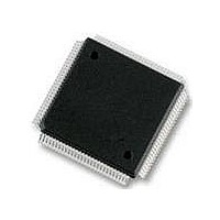
MC9S12DT256MPVE Freescale Semiconductor, MC9S12DT256MPVE Datasheet - Page 152

MC9S12DT256MPVE
Manufacturer Part Number
MC9S12DT256MPVE
Description
IC MCU 256K FLASH 25MHZ 112-LQFP
Manufacturer
Freescale Semiconductor
Series
HCS12r
Datasheet
1.S912XDG128F2MAL.pdf
(1348 pages)
Specifications of MC9S12DT256MPVE
Core Processor
HCS12
Core Size
16-Bit
Speed
25MHz
Connectivity
CAN, I²C, SCI, SPI
Peripherals
PWM, WDT
Number Of I /o
91
Program Memory Size
256KB (256K x 8)
Program Memory Type
FLASH
Eeprom Size
4K x 8
Ram Size
12K x 8
Voltage - Supply (vcc/vdd)
2.35 V ~ 5.25 V
Data Converters
A/D 8x10b
Oscillator Type
Internal
Operating Temperature
-40°C ~ 125°C
Package / Case
112-LQFP
Processor Series
S12D
Core
HCS12
Data Bus Width
16 bit
Data Ram Size
12 KB
Interface Type
CAN/I2C/SCI/SPI
Maximum Clock Frequency
25 MHz
Number Of Programmable I/os
91
Number Of Timers
1
Operating Supply Voltage
5 V to 2.5 V
Maximum Operating Temperature
+ 125 C
Mounting Style
SMD/SMT
3rd Party Development Tools
EWHCS12
Development Tools By Supplier
M68KIT912DP256
Minimum Operating Temperature
- 40 C
On-chip Adc
2 (8-ch x 10-bit)
No. Of I/o's
91
Eeprom Memory Size
4KB
Ram Memory Size
12KB
Cpu Speed
25MHz
No. Of Timers
1
No. Of Pwm Channels
8
Digital Ic Case Style
LQFP
Rohs Compliant
Yes
Lead Free Status / RoHS Status
Lead free / RoHS Compliant
Available stocks
Company
Part Number
Manufacturer
Quantity
Price
Company:
Part Number:
MC9S12DT256MPVE
Manufacturer:
Freescale Semiconductor
Quantity:
10 000
- Current page: 152 of 1348
- Download datasheet (8Mb)
Chapter 4 Analog-to-Digital Converter (ATD10B16CV4) Block Description
4.3.2.16.2
4.4
The ATD10B16C is structured in an analog and a digital sub-block.
4.4.1
The analog sub-block contains all analog electronics required to perform a single conversion. Separate
power supplies V
4.4.1.1
The sample and hold (S/H) machine accepts analog signals from the external world and stores them as
capacitor charge on a storage node.
The sample process uses a two stage approach. During the first stage, the sample amplifier is used to
quickly charge the storage node.The second stage connects the input directly to the storage node to
complete the sample for high accuracy.
When not sampling, the sample and hold machine disables its own clocks. The analog electronics continue
drawing their quiescent current. The power down (ADPU) bit must be set to disable both the digital clocks
and the analog power consumption.
The input analog signals are unipolar and must fall within the potential range of V
152
R (10-BIT)
R (10-BIT)
R (8-BIT)
R (8-BIT)
Reset
Reset
W
Figure 4-20. Right Justified, ATD Conversion Result Register x, High Byte (ATDDRxH)
W
Figure 4-21. Right Justified, ATD Conversion Result Register x, Low Byte (ATDDRxL)
Functional Description
Analog Sub-block
BIT 7 MSB
Sample and Hold Machine
Right Justified Result Data
BIT 7
0
0
0
0
7
7
DDA
and V
= Unimplemented or Reserved
= Unimplemented or Reserved
BIT 6
BIT 6
SSA
0
0
0
0
6
6
allow to isolate noise of other MCU circuitry from the analog sub-block.
MC9S12XDP512 Data Sheet, Rev. 2.21
BIT 5
BIT 5
0
0
0
0
5
5
BIT 4
BIT 4
0
0
0
0
4
4
BIT 3
BIT 3
3
0
0
0
3
0
BIT 2
BIT 2
0
0
0
0
2
2
SSA
BIT 9 MSB
Freescale Semiconductor
BIT 1
BIT 1
to VDDA.
0
0
0
1
1
BIT 8
BIT 0
BIT 0
0
0
0
0
0
Related parts for MC9S12DT256MPVE
Image
Part Number
Description
Manufacturer
Datasheet
Request
R
Part Number:
Description:
Manufacturer:
Freescale Semiconductor, Inc
Datasheet:
Part Number:
Description:
Manufacturer:
Freescale Semiconductor, Inc
Datasheet:
Part Number:
Description:
Manufacturer:
Freescale Semiconductor, Inc
Datasheet:
Part Number:
Description:
Manufacturer:
Freescale Semiconductor, Inc
Datasheet:
Part Number:
Description:
Manufacturer:
Freescale Semiconductor, Inc
Datasheet:
Part Number:
Description:
Manufacturer:
Freescale Semiconductor, Inc
Datasheet:
Part Number:
Description:
Manufacturer:
Freescale Semiconductor, Inc
Datasheet:
Part Number:
Description:
Manufacturer:
Freescale Semiconductor, Inc
Datasheet:
Part Number:
Description:
Manufacturer:
Freescale Semiconductor, Inc
Datasheet:
Part Number:
Description:
Manufacturer:
Freescale Semiconductor, Inc
Datasheet:
Part Number:
Description:
Manufacturer:
Freescale Semiconductor, Inc
Datasheet:
Part Number:
Description:
Manufacturer:
Freescale Semiconductor, Inc
Datasheet:
Part Number:
Description:
Manufacturer:
Freescale Semiconductor, Inc
Datasheet:
Part Number:
Description:
Manufacturer:
Freescale Semiconductor, Inc
Datasheet:
Part Number:
Description:
Manufacturer:
Freescale Semiconductor, Inc
Datasheet:


