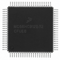
MCHC912B32CFUE8 Freescale Semiconductor, MCHC912B32CFUE8 Datasheet - Page 88

MCHC912B32CFUE8
Manufacturer Part Number
MCHC912B32CFUE8
Description
IC MCU 32K FLASH 8MHZ 80-QFP
Manufacturer
Freescale Semiconductor
Series
HC12r
Datasheet
1.MCHC912B32CFUE8.pdf
(334 pages)
Specifications of MCHC912B32CFUE8
Core Processor
CPU12
Core Size
16-Bit
Speed
8MHz
Connectivity
SCI, SPI
Peripherals
POR, PWM, WDT
Number Of I /o
63
Program Memory Size
32KB (32K x 8)
Program Memory Type
FLASH
Eeprom Size
768 x 8
Ram Size
1K x 8
Voltage - Supply (vcc/vdd)
4.5 V ~ 5.5 V
Data Converters
A/D 8x10b
Oscillator Type
External
Operating Temperature
-40°C ~ 85°C
Package / Case
80-QFP
Cpu Family
HC12
Device Core Size
16b
Frequency (max)
8MHz
Interface Type
SCI/SPI
Total Internal Ram Size
1KB
# I/os (max)
63
Operating Supply Voltage (typ)
5V
Operating Supply Voltage (max)
5.5V
Operating Supply Voltage (min)
4.5V
On-chip Adc
8-chx10-bit
Instruction Set Architecture
CISC
Operating Temp Range
-40C to 85C
Operating Temperature Classification
Industrial
Mounting
Surface Mount
Pin Count
80
Package Type
PQFP
Package
80PQFP
Family Name
HC12
Maximum Speed
8 MHz
Operating Supply Voltage
5 V
Data Bus Width
16 Bit
Number Of Programmable I/os
63
Processor Series
HC912B
Core
HC12
Data Ram Size
1 KB
Maximum Clock Frequency
8 MHz
Maximum Operating Temperature
+ 85 C
Mounting Style
SMD/SMT
3rd Party Development Tools
EWHCS12
Development Tools By Supplier
M68EVB912B32E
Minimum Operating Temperature
- 40 C
Lead Free Status / RoHS Status
Lead free / RoHS Compliant
Available stocks
Company
Part Number
Manufacturer
Quantity
Price
Company:
Part Number:
MCHC912B32CFUE8
Manufacturer:
Freescale Semiconductor
Quantity:
10 000
- Current page: 88 of 334
- Download datasheet (2Mb)
Bus Control and Input/Output (I/O)
6.3.5 Port E Data Register
Read: Anytime, if register is in the map
Write: Anytime, if register is in the map
This register is associated with external bus control signals and interrupt inputs including:
When the associated pin is not used for one of these specific functions, the pin can be used as
general-purpose I/O. The port E assignment register (PEAR) selects the function of each pin. DDRE
determines the primary direction of each port E pin when configured to be general-purpose I/O.
Some of these pins have software selectable pullups (DBE, LSTRB, R/W, and XIRQ). A single control bit
enables the pullups for all these pins which are configured as inputs. IRQ always has a pullup.
This register is not in the map in peripheral mode or expanded modes when the EME bit is set.
6.3.6 Port E Data Direction Register
Read: Anytime, if register is in the map
Write: Anytime, if register is in the map
This register determines the primary direction for each port E pin configured as general-purpose I/O.
88
•
•
•
•
•
•
•
1 = Associated pin is an output.
0 = Associated pin is a high-impedance input.
Data bus enable (DBE)
Mode select (MODB/IPIPE1 and MODA/IPIPE0)
E clock
Data size (LSTRB/TAGLO)
Read/write (R/W)
IRQ
XIRQ
Alternate function:
Address: $0009
Reset:
Read:
Write:
Address: $0008
Reset:
Read:
Write:
DDE7
Bit 7
0
Figure 6-6. Port E Data Direction Register (DDRE)
Bit 7
DBE
PE7
0
Figure 6-5. Port E Data Register (PORTE)
= Unimplemented
DDE6
6
0
MODB or
IPIPE1
M68HC12B Family Data Sheet, Rev. 9.1
PE6
6
0
DDE5
5
0
MODA or
IPIPE0
PE5
5
0
DDE4
4
0
ECLK
PE4
4
0
DDE3
3
0
LSTRB or
TAGLO
PE3
3
0
DDE2
2
0
PE2
R/W
2
0
1
0
0
PE1
IRQ
1
0
Freescale Semiconductor
Bit 0
0
0
XIRQ
Bit 0
PE0
0
Related parts for MCHC912B32CFUE8
Image
Part Number
Description
Manufacturer
Datasheet
Request
R
Part Number:
Description:
Manufacturer:
Freescale Semiconductor, Inc
Datasheet:
Part Number:
Description:
Manufacturer:
Freescale Semiconductor, Inc
Datasheet:
Part Number:
Description:
Manufacturer:
Freescale Semiconductor, Inc
Datasheet:
Part Number:
Description:
Manufacturer:
Freescale Semiconductor, Inc
Datasheet:
Part Number:
Description:
Manufacturer:
Freescale Semiconductor, Inc
Datasheet:
Part Number:
Description:
Manufacturer:
Freescale Semiconductor, Inc
Datasheet:
Part Number:
Description:
Manufacturer:
Freescale Semiconductor, Inc
Datasheet:
Part Number:
Description:
Manufacturer:
Freescale Semiconductor, Inc
Datasheet:
Part Number:
Description:
Manufacturer:
Freescale Semiconductor, Inc
Datasheet:
Part Number:
Description:
Manufacturer:
Freescale Semiconductor, Inc
Datasheet:
Part Number:
Description:
Manufacturer:
Freescale Semiconductor, Inc
Datasheet:
Part Number:
Description:
Manufacturer:
Freescale Semiconductor, Inc
Datasheet:
Part Number:
Description:
Manufacturer:
Freescale Semiconductor, Inc
Datasheet:
Part Number:
Description:
Manufacturer:
Freescale Semiconductor, Inc
Datasheet:
Part Number:
Description:
Manufacturer:
Freescale Semiconductor, Inc
Datasheet:


